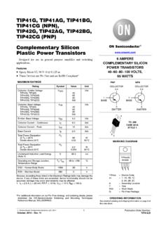
Transcription of TIP140, TIP141, TIP142, TIP145, TIP146, TIP147 ...
1 Semiconductor Components Industries, LLC, 2012 May, 2012 Rev. 61 Publication Order Number: tip140 /DTIP140, tip141 , tip142 ,(NPN); tip145 , TIP146, TIP147 , (PNP)Darlington ComplementarySilicon Power TransistorsDesigned for general purpose amplifier and low frequencyswitching High DC Current Gain Min hFE= 1000 @ IC = A, VCE = 4 V Collector Emitter Sustaining Voltage @ 30 mA VCEO(sus)= 60 Vdc (Min) tip140 , tip145 = 80 Vdc (Min) tip141 , tip146 = 100 Vdc (Min) tip142 , TIP147 Monolithic Construction with Built In Base Emitter Shunt Resistor These are Pb Free Devices*MAXIMUM RATINGSR atingSymbolTIP140 tip145 tip141 tip146 tip142 TIP147 UnitCollector Emitter VoltageVCEO6080100 VdcCollector Base VoltageVCB6080100 VdcEmitter Base Current Continuous Peak (Note 1)IC1015 AdcBase Current Power Dissipation@ TC = 25_CPD125 WOperating and Storage Junction Temperature RangeTJ, Tstg 65 to +150_CTHERMAL CHARACTERISTICSC haracteristicSymbolMaxUnitThermal Resistance,Junction to C/WThermal Resistance,Junction to C/WStresses exceeding Maximum Ratings may damage the device.
2 MaximumRatings are stress ratings only. Functional operation above the RecommendedOperating Conditions is not implied. Extended exposure to stresses above theRecommended Operating Conditions may affect device 5 ms, v 10% Duty Cycle.*For additional information on our Pb Free strategy and soldering details, pleasedownload the ON Semiconductor Soldering and Mounting TechniquesReference Manual, AMPEREDARLINGTONCOMPLEMENTARY SILICONPOWER TRANSISTORS60 100 VOLTS, 125 WATTSSee detailed ordering and shipping information in the packagedimensions section on page 2 of this data 93 (TO 218)CASE 340 DSTYLE 1TO 247 CASE 340 LSTYLE 3 NOTE: Effective June 2012 this device willbe available only in the TO 247package. Reference FPCN# , tip141 , tip142 , (NPN); tip145 , tip146 , TIP147 , (PNP) DIAGRAMSAYWWGTIP14xTIP14xAYWWG1 BASE2 COLLECTOR3 EMITTERTIP14x= Device CodeA= Assembly LocationY= YearWW= Work WeekG=Pb Free Package1 BASE2 COLLECTOR3 EMITTERTO 247TO 218 DARLINGTON SCHEMATICSBASEEMITTERCOLLECTOR k 40 BASEEMITTERCOLLECTOR k 40 NPNTIP140 tip141 tip142 PNPTIP145 tip146 TIP147 ORDERING INFORMATIOND evicePackageShippingTIP140 GSOT 93 (TO 218)(Pb Free)30 Units / RailTIP141 GSOT 93 (TO 218)(Pb Free)30 Units / RailTIP142 GSOT 93 (TO 218)(Pb Free)30 Units / RailTIP145 GSOT 93 (TO 218)(Pb Free)30 Units / RailTIP146 GSOT 93 (TO 218)(Pb Free)30 Units / RailTIP147 GSOT 93 (TO 218)(Pb Free)30 Units / RailTIP140 GTO 247(Pb Free)30 Units / RailTIP141 GTO 247(Pb Free)30 Units / RailTIP142 GTO 247(Pb Free)30 Units / RailTIP145 GTO 247(Pb Free)30 Units / RailTIP146 GTO 247(Pb Free)
3 30 Units / RailTIP147 GTO 247(Pb Free)30 Units / RailTIP140, tip141 , tip142 , (NPN); tip145 , tip146 , TIP147 , (PNP) ELECTRICAL CHARACTERISTICS (TC = 25_C unless otherwise noted) Characteristic Symbol Min Typ Max Unit OFF CHARACTERISTICS Collector Emitter Sustaining Voltage (Note 2)(IC = 30 mA, IB = 0) tip140 , tip145 tip141 , tip146 tip142 , TIP147 VCEO(sus) 6080100 Vdc Collector Cutoff Current(VCE = 30 Vdc, IB = 0) tip140 , tip145 (VCE = 40 Vdc, IB = 0) tip141 , tip146 (VCE = 50 Vdc, IB = 0)
4 tip142 , TIP147 ICEO mA Collector Cutoff Current(VCB = 60 V, IE = 0) tip140 , tip145 (VCB = 80 V, IE = 0) tip141 , tip146 (VCB = 100 V, IE = 0) tip142 , TIP147 ICBO mA Emitter Cutoff Current (VBE = V) IEBO 2 0 mA ON CHARACTERISTICS (Note 2) DC Current Gain(IC = A, VCE = V)(IC = 10 A, VCE = V) hFE 1000500 Collector Emitter Saturation Voltage(IC = A, IB = 10 mA)(IC = 10 A, IB = 40 mA) VCE(sat) Vdc Base Emitter Saturation Voltage(IC = 10 A, IB = 40 mA) VBE(sat) Vdc Base Emitter On Voltage(IC = 10 A, VCE = Vdc) VBE(on) Vdc SWITCHING CHARACTERISTICS Resistive Load (See Figure 1)
5 Delay Time (VCC = 30 V, IC = A,IB = 20 mA, Duty Cycle v ,IB1 = IB2, RC & RB Varied, TJ = 25_C) td ms Rise Time tr ms Storage Time ts ms Fall Time tf ms2. Pulse Test: Pulse Width = 300 ms, Duty Cycle v 1. Switching Times Test 2. Switching TimesIC, COLLECTOR CURRENT (AMP)t, TIME ( s) @ VBE(off) = 0V2approx+12 Vtr, tf 10 nsDUTY CYCLE = ms0RB51D1+ VVCC- 30 VRCTUT k 40 SCOPEfor td and tr, D1 is disconnectedand V2 = 0RB & RC VARIED TO OBTAIN DESIRED CURRENT LEVELSD1, MUST BE FAST RECOVERY TYPE, eg: 1N5825 USED ABOVE IB 100 mA MSD6100 USED BELOW IB 100 mAVCC = 30 VIC/IB = 250IB1 = IB2TJ = 25 CFor NPN test circuit reverse diode and voltage , tip141 , tip142 , (NPN); tip145 , tip146 , TIP147 , (PNP) (SAT), COLLECTOR-EMITTER SATURATION VOLTAGE (VOLTS)VBE, BASE-EMITTER VOLTAGE (VOLTS)VBE, BASE-EMITTER VOLTAGE (VOLTS) 3.
6 DC Current Gain versus Collector CurrentIC, COLLECTOR CURRENT (AMPS) , DC CURRENT GAINVCE = , tip141 , tip142 PNPTIP145, tip146 , TIP147 Figure 4. Collector Emitter Saturation 75TJ, JUNCTION TEMPERATURE ( C) = 10 A, IB = 75TJ, JUNCTION TEMPERATURE ( C)- 5. Base Emitter Voltage20001000TJ = 150 C25 C- 55 CIC, COLLECTOR CURRENT (AMPS)hFE, DC CURRENT GAINTJ, JUNCTION TEMPERATURE ( C)TJ, JUNCTION TEMPERATURE ( C)12520,000100020003000500010, (SAT), COLLECTOR-EMITTER SATURATION VOLTAGE (VOLTS) 50- 50- 75- CTJ = 150 C100 C25 C- 55 CVCE = VIC = A, IB = 10 mAIC = A, IB = mAIC = 10 A, IB = mAIC = A, IB = 10 mAIC = A, IB = mAVCE = VIC = 10 AVCE = VIC = 10 ATYPICAL CHARACTERISTICSTIP140, tip141 , tip142 , (NPN); tip145 , tip146 , TIP147 , (PNP) REGION SAFE OPERATING AREAT here are two limitations on the power handling ability ofa transistor: average junction temperature and secondbreakdown.
7 Safe operating area curves indicate IC VCElimits of the transistor that must be observed for reliableoperation; , the transistor must not be subjected to greaterdissipation than the curves data of Figure 6 is based on TJ(pk) = 150_C; TC isvariable depending on conditions. At high casetemperatures, thermal limitations will reduce the power thatcan be handled to values less than the limitations imposed bysecond BREAKDOWN LIMITBONDING WIRE LIMITTHERMAL LIMITATION @ TC = 25 CFigure 6. Active Region Safe Operating AreadcVCE, COLLECTOR-EMITTER VOLTAGE (VOLTS) , COLLECTOR CURRENT (AMP) (mA) TJ = 150 C5030 tip140 , , 146 tip142 , 147IC, COLLECTOR CURRENT (AMPS) 7. Unclamped Inductive LoadL, UNCLAMPED INDUCTIVE LOAD (mH) kRBB2= 100 VBB2 = 0 VBB1 = 10 VTUTVCE MONITOR100 mHVCC = 20 VICMONITORRS = CIRCUITNOTE 1: Input pulse width is increased until ICM = 2: For NPN test circuit reverse AVCE(sat)- 20 VCOLLECTORVOLTAGEV(BR)CERw ms (SEE NOTE 1) V0100 ms0 VOLTAGE AND CURRENT WAVEFORMSF igure 8.
8 Inductive LoadTIP140, tip141 , tip142 , (NPN); tip145 , tip146 , TIP147 , (PNP) , POWER DISSIPATION (WATTS)PNPNPNF igure 9. Magnitude of Common EmitterSmall Signal Short Circuit ForwardCurrent Transfer Ratiof, FREQUENCY (MHz) = 10 VIC = ATJ = 25 10. Free Air Temperature Power DeratingTA, FREE-AIR TEMPERATURE ( C)04080120160200hfe, SMALL-SIGNAL FORWARD CURRENTTRANSFER RATIO205070 PNPNPNTIP140, tip141 , tip142 , (NPN); tip145 , tip146 , TIP147 , (PNP) DIMENSIONSSOT 93 (TO 218)CASE 340D 02 ISSUE ESTYLE 1:PIN 1. BASE2. COLLECTOR3. EMITTER4. COLLECTORADVGKSLUBQ1234 NOTES:1. DIMENSIONING AND TOLERANCING PER , CONTROLLING DIMENSION: 247 CASE 340L 02 ISSUE ( )MYQSJHC4123 T B Y NOTES:1. DIMENSIONING AND TOLERANCING PER , CONTROLLING DIMENSION: PL3 ( )MTBM Q LDIMMINMAXMIN 3:PIN 1. BASE 2. COLLECTOR 3.
9 EMITTER 4. COLLECTORTIP140, tip141 , tip142 , (NPN); tip145 , tip146 , TIP147 , (PNP) Semiconductor and are registered trademarks of Semiconductor Components Industries, LLC (SCILLC). SCILLC reserves the right to make changes without further noticeto any products herein. SCILLC makes no warranty, representation or guarantee regarding the suitability of its products for any particular purpose, nor does SCILLC assume any liabilityarising out of the application or use of any product or circuit, and specifically disclaims any and all liability, including without limitation special, consequential or incidental damages. Typical parameters which may be provided in SCILLC data sheets and/or specifications can and do vary in different applications and actual performance may vary over time. Alloperating parameters, including Typicals must be validated for each customer application by customer s technical experts.
10 SCILLC does not convey any license under its patent rightsnor the rights of others. SCILLC products are not designed, intended, or authorized for use as components in systems intended for surgical implant into the body, or other applicationsintended to support or sustain life, or for any other application in which the failure of the SCILLC product could create a situation where personal injury or death may occur. ShouldBuyer purchase or use SCILLC products for any such unintended or unauthorized application, Buyer shall indemnify and hold SCILLC and its officers, employees, subsidiaries, affiliates,and distributors harmless against all claims, costs, damages, and expenses, and reasonable attorney fees arising out of, directly or indirectly, any claim of personal injury or deathassociated with such unintended or unauthorized use, even if such claim alleges that SCILLC was negligent regarding the design or manufacture of the part.