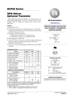
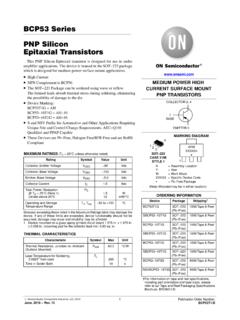
Transcription of TIP41A - Complementary Silicon Plastic Power …
1 Semiconductor Components Industries, LLC, 2014 October, 2014 Rev. 111 Publication Order Number: TIP41A /DTIP41G, TIP41AG, TIP41BG,TIP41CG (NPN),TIP42G, TIP42AG, TIP42BG,TIP42CG (PNP) Complementary SiliconPlastic Power TransistorsDesigned for use in general purpose amplifier and Epoxy Meets UL 94 V 0 @ in These Devices are Pb Free and are RoHS Compliant*MAXIMUM RATINGSR atingSymbolValueUnitCollector Emitter VoltageTIP41G, TIP42 GTIP41AG, TIP42 AGTIP41BG, TIP42 BGTIP41CG, TIP42 CGVCEO406080100 VdcCollector Base VoltageTIP41G, TIP42 GTIP41AG, TIP42 AGTIP41BG, TIP42 BGTIP41CG, TIP42 CGVCB406080100 VdcEmitter Base Current Current PeakICM10 AdcBase Power Dissipation@ TC = 25 CDerate above 25 CTotal Power Dissipation@ TA = 25 CDerate above 25 CUnclamped Inductive Load Energy(Note 1) and Storage Junction,Temperature RangeTJ, Tstg 65 to +150 CESD Human Body ModelHBM3 BVESD Machine ModelMMCVS tresses exceeding those listed in the Maximum Ratings table may damage thedevice.
2 If any of these limits are exceeded, device functionality should not beassumed, damage may occur and reliability may be IC = A, L = 20 mH, = 10 Hz, VCC = 10 V, RBE = 100 W.*For additional information on our Pb Free strategy and soldering details, pleasedownload the ON Semiconductor Soldering and Mounting TechniquesReference Manual, 220 CASE 221 ASTYLE 1 MARKING DIAGRAM6 AMPERECOMPLEMENTARY SILICONPOWER TRANSISTORS40 60 80 100 VOLTS,65 Device Codexx= 1, 1A, 1B, 1C2, 2A, 2B, 2CA= Assembly LocationY= YearWW= Work WeekG=Pb Free PackageTIP4xxGAYWWSee detailed ordering and shipping information on page 6 ofthis data INFORMATION1 BASE3 EMITTERCOLLECTOR2,41 BASE3 EMITTERCOLLECTOR2,4 NPNPNPTIP41G, TIP41AG, TIP41BG, TIP41CG (NPN)
3 , TIP42G, TIP42AG, TIP42BG,TIP42CG (PNP) CHARACTERISTICSC haracteristicSymbolMaxUnitThermal Resistance, Junction to C/WThermal Resistance, Junction to AmbientRqJA57 C/WELECTRICAL CHARACTERISTICS (TC = 25 C unless otherwise noted)CharacteristicSymbolMinMaxUnitOFF CHARACTERISTICSC ollector Emitter Sustaining Voltage (Note 2)(IC = 30 mAdc, IB = 0)TIP41G, TIP42 GTIP41AG, TIP42 AGTIP41BG, TIP42 BGTIP41CG, TIP42 CGVCEO(sus)406080100 VdcCollector Cutoff Current(VCE = 30 Vdc, IB = 0)TIP41G, TIP41AG, TIP42G, TIP42AG(VCE = 60 Vdc, IB = 0)TIP41BG, TIP41CG, TIP42BG, TIP42 CGICEO Cutoff Current(VCE = 40 Vdc, VEB = 0)TIP41G, TIP42G(VCE = 60 Vdc, VEB = 0)TIP41AG, TIP42AG(VCE = 80 Vdc, VEB = 0)TIP41BG, TIP42BG(VCE = 100 Vdc, VEB = 0)TIP41CG, TIP42 CGICES 400400400400mAdcEmitter Cutoff Current (VBE = Vdc, IC = 0)IEBO CHARACTERISTICS (Note 2)DC Current Gain(IC = Adc, VCE = Vdc)(IC = Adc, VCE = Vdc)hFE3015 75 Collector Emitter Saturation Voltage(IC = Adc, IB = 600 mAdc)VCE(sat) Emitter On Voltage(IC = Adc, VCE = Vdc)VBE(on) CHARACTERISTICSC urrent Gain Bandwidth Product(IC = 500 mAdc, VCE = 10 Vdc, ftest = MHz)
4 MHzSmall Signal Current Gain(IC = Adc, VCE = 10 Vdc, f = kHz)hfe20 Product parametric performance is indicated in the Electrical Characteristics for the listed test conditions, unless otherwise noted. Productperformance may not be indicated by the Electrical Characteristics if operated under different Pulse Test: Pulse Width 300 ms, Duty Cycle , TIP41AG, TIP41BG, TIP41CG (NPN), TIP42G, TIP42AG, TIP42BG,TIP42CG (PNP) 1. Power DeratingT, TEMPERATURE ( C)0100020160406060804014080 Figure 2. Switching Time Test 3. Turn On TimeIC, COLLECTOR CURRENT (AMP) = 25 CVCC = 30 VIC/IB = 10t, TIME ( s) @ VBE(off) , Power DISSIPATION (WATTS) +11 V25 ms0- VRB- 4 VD1 SCOPEVCC+ 30 VRCtr, tf 10 nsDUTY CYCLE = and RC VARIED TO OBTAIN DESIRED CURRENT LEVELSD1 MUST BE FAST RECOVERY TYPE.
5 1N5825 USED ABOVE IB 100 mA MSD6100 USED BELOW IB 100 , TIP41AG, TIP41BG, TIP41CG (NPN), TIP42G, TIP42AG, TIP42BG,TIP42CG (PNP) , TIME (ms) (t), TRANSIENT THERMAL RESISTANCE (NORMALIZED) (t) = r(t) RqJCRqJC = C/W MAXD CURVES APPLY FOR POWERPULSE TRAIN SHOWNREAD TIME AT t1TJ(pk) - TC = P(pk) ZqJC(t)P(pk)t1t2 SINGLE kD = CYCLE, D = t1/t2 Figure 4. Thermal Response , COLLECTOR-EMITTER VOLTAGE (VOLTS) 5. Active Region Safe Operating BREAKDOWN LTDBONDING WIRE LTDTHERMAL LIMITATION @ TC = 25 C(SINGLE PULSE) , COLLECTOR CURRENT (AMP) msCURVES APPLY BELOW RATED msTJ = 150 CTIP41, TIP42 TIP41A , TIP42 ATIP41B, TIP42 BTIP41C, TIP42 CThere are two limitations on the Power handling ability ofa transistor: average junction temperature and secondbreakdown.
6 Safe operating area curves indicate IC VCElimits of the transistor that must be observed for reliableoperation; , the transistor must not be subjected to greaterdissipation than the curves data of Figure 5 is based on TJ(pk) = 150 C; TC isvariable depending on conditions. Second breakdown pulselimits are valid for duty cycles to 10% provided TJ(pk) 150 C. TJ(pk) may be calculated from the data in Figure high case temperatures, thermal limitations will reducethe Power that can be handled to values less than thelimitations imposed by second , COLLECTOR CURRENT (AMP)Figure 6.
7 Turn Off , TIME ( s) , REVERSE VOLTAGE (VOLTS)Figure 7. Capacitance300C, CAPACITANCE (pF)2001007050303050TJ = 25 CVCC = 30 VIC/IB = 10IB1 = = 25 CTIP41G, TIP41AG, TIP41BG, TIP41CG (NPN), TIP42G, TIP42AG, TIP42BG,TIP42CG (PNP) , COLLECTOR-EMITTER VOLTAGE (VOLTS)TJ, JUNCTION TEMPERATURE ( C)103- M100 k10 kIB, BASE CURRENT (mA)IC, COLLECTOR CURRENT (AMP)hFE, DC CURRENT GAINF igure 8. DC Current GainFigure 9. Collector Saturation RegionIC, COLLECTOR CURRENT (AMP) , BASE-EMITTER VOLTAGE (VOLTS)Figure 10. On VoltagesVCE = CTJ = 150 C- 55 , COLLECTOR CURRENT (AMP) + = A20608010012016014040V, VOLTAGE (VOLTS)TJ = 25 (sat) @ IC/IB = 10 VBE @ VCE = VVCE(sat) @ IC/IB = 10V, TEMPERATURE COEFFICIENTS (mV/ C) + + + + *APPLIES FOR IC/IB hFE/4* qVC FOR VCE(sat)qVB FOR VBEF igure 11.
8 Temperature Coefficients, COLLECTOR CURRENT ( A) IC- - + + + + + + 12. Collector Cut Off RegionFigure 13. Effects of Base Emitter ResistanceVCE = 30 VTJ = 150 C100 C25 CREVERSEFORWARDIC = ICESRBE, EXTERNAL BASE-EMITTER RESISTANCE (OHMS)VCE = 30 VIC = 10 x ICESIC ICESIC = 2 x ICES(TYPICAL ICES VALUESOBTAINED FROM FIGURE 12) + 25 C to + 150 C- 55 C to + 25 C+ 25 C to + 150 C- 55 C to + 25 C+ = 25 CTIP41G, TIP41AG, TIP41BG, TIP41CG (NPN), TIP42G, TIP42AG, TIP42BG,TIP42CG (PNP) INFORMATIOND evicePackageShippingTIP41 GTO 220(Pb Free)50 Units / RailTIP41 AGTO 220(Pb Free)50 Units / RailTIP41 BGTO 220(Pb Free)50 Units / RailTIP41 CGTO 220(Pb Free)50 Units / RailTIP42 GTO 220(Pb Free)
9 50 Units / RailTIP42 AGTO 220(Pb Free)50 Units / RailTIP42 BGTO 220(Pb Free)50 Units / RailTIP42 CGTO 220(Pb Free)50 Units / RailTIP41G, TIP41AG, TIP41BG, TIP41CG (NPN), TIP42G, TIP42AG, TIP42BG,TIP42CG (PNP) DIMENSIONSTO 220 CASE 221A 09 ISSUE AHNOTES:1. DIMENSIONING AND TOLERANCING PER , CONTROLLING DIMENSION: DIMENSION Z DEFINES A ZONE WHERE ALLBODY AND LEAD IRREGULARITIES MINMAXMIN T CSTURJSTYLE 1:PIN 1. BASE2. COLLECTOR3. EMITTER4. COLLECTORON Semiconductor and the are registered trademarks of Semiconductor Components Industries, LLC (SCILLC) or its subsidiaries in the United States and/or other owns the rights to a number of patents, trademarks, copyrights, trade secrets, and other intellectual property.
10 A listing of SCILLC s product/patent coverage may be accessedat SCILLC reserves the right to make changes without further notice to any products herein. SCILLC makes no warranty, representationor guarantee regarding the suitability of its products for any particular purpose, nor does SCILLC assume any liability arising out of the application or use of any product or circuit, andspecifically disclaims any and all liability, including without limitation special, consequential or incidental damages. Typical parameters which may be provided in SCILLC data sheetsand/or specifications can and do vary in different applications and actual performance may vary over time.
