Transcription of V R D -30V = -10V -3
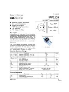
1 PD - 93967A. PROVISIONAL. IRLML5203. HEXFET Power MOSFET. l Ultra Low On-Resistance VDSS RDS(on) max (mW) ID. l P-Channel MOSFET -30V 98@VGS = -10V l Surface Mount 165@VGS = l Available in Tape & Reel l Low Gate Charge Description These P-channel MOSFETs from International Rectifier G 1. utilize advanced processing techniques to achieve the extremely low on-resistance per silicon area. This benefit provides the designer with an extremely efficient 3 D. device for use in battery and load management applications. S 2. A thermally enhanced large pad leadframe has been Micro3TM. incorporated into the standard SOT-23 package to produce a HEXFET Power MOSFET with the industry's smallest footprint. This package, dubbed the Micro3TM, is ideal for applications where printed circuit board space is at a premium.
2 The low profile (< ) of the Micro3 allows it to fit easily into extremely thin application environments such as portable electronics and PCMCIA cards. The thermal resistance and power dissipation are the best available. Absolute Maximum Ratings Parameter Max. Units VDS Drain- Source Voltage -30 V. ID @ TA = 25 C Continuous Drain Current, VGS @ -10V ID @ TA= 70 C Continuous Drain Current, VGS @ -10V A. IDM Pulsed Drain Current -24. PD @TA = 25 C Power Dissipation W. PD @TA = 70 C Power Dissipation Linear Derating Factor 10 mW/ C. VGS Gate-to-Source Voltage 20 V. TJ, TSTG Junction and Storage Temperature Range -55 to + 150 C. Thermal Resistance Parameter Max. Units R JA Maximum Junction-to-Ambient 100 C/W. 1. 04/30/03. IRLML5203 PROVISIONAL.
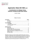
3 Electrical Characteristics @ TJ = 25 C (unless otherwise specified). Parameter Min. Typ. Max. Units Conditions V(BR)DSS Drain-to-Source Breakdown Voltage -30 V VGS = 0V, ID = -250 A. V(BR)DSS/ TJ Breakdown Voltage Temp. Coefficient V/ C Reference to 25 C, I D = -1mA. 98 VGS = -10V, ID = . RDS(on) Static Drain-to-Source On-Resistance m . 165 VGS = , ID = . VGS(th) Gate Threshold Voltage V VDS = VGS, ID = -250 A. gfs Forward Transconductance S VDS = -10V, ID = VDS = -24V, VGS = 0V. IDSS Drain-to-Source Leakage Current A. VDS = -24V, VGS = 0V, TJ = 70 C. Gate-to-Source Forward Leakage -100 VGS = -20V. I GSS nA. Gate-to-Source Reverse Leakage 100 VGS = 20V. Qg Total Gate Charge 14 ID = Qgs Gate-to-Source Charge nC VDS = -24V.
4 Qgd Gate-to-Drain ("Miller") Charge VGS = -10V . td(on) Turn-On Delay Time 12 VDD = -15V . tr Rise Time 18 ID = ns td(off) Turn-Off Delay Time 88 R G = . tf Fall Time 52 VGS = -10V. Ciss Input Capacitance 510 VGS = 0V. Coss Output Capacitance 71 pF VDS = -25V. Crss Reverse Transfer Capacitance 43 = Source-Drain Ratings and Characteristics Parameter Min. Typ. Max. Units Conditions IS Continuous Source Current MOSFET symbol D. (Body Diode) showing the A. ISM Pulsed Source Current integral reverse G. -24. (Body Diode) p-n junction diode. S. VSD Diode Forward Voltage V TJ = 25 C, IS = , VGS = 0V . trr Reverse Recovery Time 17 26 ns TJ = 25 C, IF = Qrr Reverse Recovery Charge 12 18 nC di/dt = -100A/ s . Notes: Repetitive rating; pulse width limited by Surface mounted on FR-4 board, t 5sec.
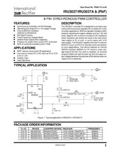
5 Max. junction temperature. Pulse width 400 s; duty cycle 2%. 2 PROVISIONAL IRLML5203. 100 VGS 100. VGS. TOP -15V TOP -15V. -10V -10V. -I D , Drain-to-Source Current (A). -I D , Drain-to-Source Current (A). 10 BOTTOM BOTTOM 10. 1. 1. 20 s PULSE WIDTH 20 s PULSE WIDTH. TJ = 25 C TJ = 150 C. 1 10 100 1 10 100. -VDS , Drain-to-Source Voltage (V) -VDS , Drain-to-Source Voltage (V). Fig 1. Typical Output Characteristics Fig 2. Typical Output Characteristics 100 ID = RDS(on) , Drain-to-Source On Resistance -I D , Drain-to-Source Current (A). 10. (Normalized). TJ = 150 C 1. TJ = 25 C. V DS = -15V. 20 s PULSE WIDTH VGS = -10V. -60 -40 -20 0 20 40 60 80 100 120 140 160. -VGS , Gate-to-Source Voltage (V) TJ , Junction Temperature ( C).
6 Fig 3. Typical Transfer Characteristics Fig 4. Normalized On-Resistance Vs. Temperature 3. IRLML5203 PROVISIONAL. 800 20. VGS = 0V, f = 1 MHz ID = Ciss = Cgs + Cgd , Cds SHORTED VDS =-24V. -VGS , Gate-to-Source Voltage (V). Crss = Cgd VDS =-15V. Coss = Cds + Cgd 16. 600. C, Capacitance (pF). Ciss 12. 400. 8. 200. 4. Coss Crss 0 0. 1 10 100 0 4 8 12 16. -VDS , Drain-to-Source Voltage (V) QG , Total Gate Charge (nC). Fig 5. Typical Capacitance Vs. Fig 6. Typical Gate Charge Vs. Drain-to-Source Voltage Gate-to-Source Voltage 100 100. OPERATION IN THIS AREA LIMITED. BY RDS(on). -ISD , Reverse Drain Current (A). -II D , Drain Current (A). 10us 10 10. TJ = 150 C. 100us 1ms 1 1. TJ = 25 C. 10ms TA = 25 C. TJ = 150 C. V GS = 0 V Single Pulse 1 10 100.
7 -VSD ,Source-to-Drain Voltage (V) -VDS , Drain-to-Source Voltage (V). Fig 7. Typical Source-Drain Diode Fig 8. Maximum Safe Operating Area Forward Voltage 4 PROVISIONAL IRLML5203. RD. VDS. VGS. RG. -ID , Drain Current (A). - + VDD. VGS. Pulse Width 1 s Duty Factor %. Fig 10a. Switching Time Test Circuit td(on) tr t d(off) tf VGS. 10%. 25 50 75 100 125 150. TC , Case Temperature ( C). 90%. Fig 9. Maximum Drain Current Vs. VDS. Case Temperature Fig 10b. Switching Time Waveforms 1000. Thermal Response (Z thJA ). 100. D = 10 PDM. t1. 1 t2. SINGLE PULSE. (THERMAL RESPONSE). Notes: 1. Duty factor D = t 1 / t 2. 2. Peak T J = P DM x Z thJA + TA. 1 10. t1 , Rectangular Pulse Duration (sec). Fig 11. Maximum Effective Transient Thermal Impedance, Junction-to-Ambient 5.
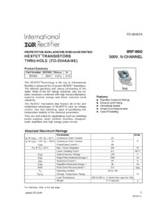
8 IRLML5203 PROVISIONAL. RDS(on) , Drain-to -Source On Resistance ( ). RDS (on) , Drain-to-Source On Resistance ( ). VGS = ID = VGS = -10V. -V GS, Gate -to -Source Voltage (V) 0 4 8 12 16. -I D , Drain Current (A). Fig 11. Typical On-Resistance Vs. Gate Fig 12. Typical On-Resistance Vs. Drain Voltage Current Current Regulator Same Type as 50K . QG 12V .2 F..3 F. - QGS QGD +VDS. VGS. VG. -3mA. IG ID. Charge Current Sampling Resistors Fig 13a. Basic Gate Charge Waveform Fig 13b. Gate Charge Test Circuit 6 PROVISIONAL IRLML5203. 30. -VGS(th) , Variace ( V ). 20. ID = -250 A. Power (W). 10. 0. -75 -50 -25 0 25 50 75 100 125 150 T J , Temperature ( C ) Time (sec). Fig 14. Threshold Voltage Vs. Temperature Fig 15. Typical Power Vs.
9 Time 7. IRLML5203 PROVISIONAL. Micro3TM Package Outline Dimensions are shown in millimeters (inches). D LEAD ASSIGNMENTS INCHES MILLIMETERS. 3 DIM. -B- 1 - GATE MIN MAX MIN MAX. 2 - SOURCE A .032 .044 3 - DRAIN A1 .001 .004 3 3 B .015 .021 E H. C .004 .006 -A- ( .008 ) M A M. 1 2 D .105 .120 e .0750 BASIC BASIC. e1 .0375 BASIC BASIC. e E .047 .055 H .083 .098 e1. L .005 .010 0 8 0 8 . A . MINIMUM RECOMMENDED FOOTPRINT. -C- (.003) ( .031 ). A1 L C 3X. B 3X. 3X 3X (.004) M C AS B S ( .035 ) 3X ( .079 ). NOTES: 1. DIMENSIONING & TOLERANCING PER ANSI 2. CONTROLLING DIMENSION : INCH. ( .037 ). 3 DIMENSIONS DO NOT INCLUDE MOLD FLASH. 2X. 8 PROVISIONAL IRLML5203. Part Marking Information Micro3TM. Notes : T his part marking information applies to devices produced before 02/26/2001.
10 WW = (1-26) IF PRECEDED BY LAS T DIGIT OF CALENDAR YEAR. EXAMPLE: T HIS IS AN IRLML6302. WORK. YEAR Y WEEK W. 2001 1 01 A. PART NUMBER. 2002 2 02 B. 2003 3 03 C. 1994 4 04 D. DATE 1995 5. CODE 1996 6. 1997 7. 1998 8. 1999 9. 2000 0 24 X. PART NUMBER CODE REFERENCE: 25 Y. 1A = IRLML2402 26 Z. 1B = IRLML2803. WW = (27-52) IF PRECEDED BY A LETT ER. 1C = IRLML6302. 1D = IRLML5103 WORK. YEAR Y WEEK W. 1E = IRLML6402. 1F = IRLML6401 2001 A 27 A. 2002 B 28 B. 1G = IRLML2502. 2003 C 29 C. 1H = IRLML5203 1994 D 30 D. 1995 E. 1996 F. DAT E CODE EXAMPLES: 1997 G. 1998 H. YWW = 9503 = 5C 1999 J. YWW = 9532 = EF 2000 K 50 X. 51 Y. 52 Z. Notes : T his part marking information applies to devices produced after 02/26/2001. W = (1-26) IF PRECE DED BY LAS T DIGIT OF CALENDAR YEAR.