Example: bankruptcy
FDS6675 - onsemi.com
FDS6675 Single P-Channel, Logic Level, PowerTrench TM MOSFET Features Absolute Maximum Ratings T A = 25 o C unless otherwise noted Symbol Parameter FDS6675 Units V DSS Drain-Source Voltage -30 V V GSS Gate-Source Voltage ± 20 V I D Drain Current - Continuous (Note 1a)-11 A - Pulsed -50 P D Power Dissipation for Single Operation (Note 1a) 2.5 W (Note 1b) 1.2 (Note 1c) 1 T J,T STG …
Tags:
Information
Domain:
Source:
Link to this page:
Documents from same domain

BCP56T1 - NPN Silicon Epitaxial Transistor
www.onsemi.com© Semiconductor Components Industries, LLC, 2016 March, 2018 − Rev. 14 1 Publication Order Number: BCP56T1/D BCP56 Series NPN Silicon Epitaxial Transistor These NPN Silicon Epitaxial transistors are designed for use in

AN1040/D Mounting Considerations For Power …
www.onsemi.comSemiconductor Components Industries, LLC, 2001 May, 2001 – Rev. 3 1 Publication Order Number: AN1040/D AN1040/D Mounting Considerations For Power Semiconductors

Corporate Fact Sheet - ON Semiconductor
www.onsemi.comCompany Profile ON Semiconductor (Nasdaq: ON) is driving energy efficient innovations, empowering customers to reduce global energy use. The company is a leading supplier of semiconductor-based

AND8231 - Circuit Configuration Options for TVS …
www.onsemi.comAND8231/D www.onsemi.com 2 Avalanche TVS Diodes Avalanche diodes are a good TVS device for applications that require power line surge immunity and ESD protection.

BCP53 Series PNP Silicon Epitaxial Transistors
www.onsemi.comBCP53 Series www.onsemi.com 3 TYPICAL CHARACTERISTICS Figure 1. Collector Emitter Saturation Voltage vs. Collector Current Figure 2. DC Current Gain vs. Collector

AND8299 - EMC Tests and PCB Guidelines for …
www.onsemi.comAND8299 - EMC Tests and PCB Guidelines for Automotive Linear Regulators

BSS138 N-Channel Logic Level Enhancement Mode …
www.onsemi.com2005 Semiconductor Components Industries, LLC. September-2017, Rev. 3 Publication Order Number: BSS138/D BSS138 N-Channel Logic Level Enhancement Mode Field Effect Transistor

TND310 ON Semiconductor Device Nomenclature
www.onsemi.comThis document contains the device nomenclature breakdown (also referred to as the part number decoder, product naming convention, or part naming convention) for …

LP2950 - 100 mA, Low Power Low Dropout Voltage …
www.onsemi.comLP2950, LP2951, NCV2951 www.onsemi.com Dropout Voltage V 0 in LP2950/LP2951 BIAS CURRENT (mA) I = 25°C V

2018 PHILIPPINES BENEFITS SUMMARY - ON …
www.onsemi.com2018 PHILIPPINES BENEFITS SUMMARY Employees are eligible for most benefits program on the first day of employment. Holidays: Ten (10) paid national regular holidays and Eight (8) national special holidays per year as provided
Related documents
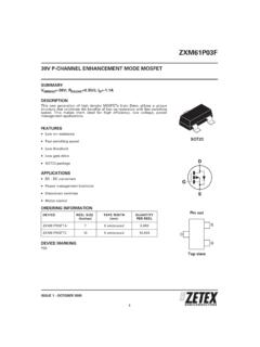
ZXM61P03F 30V P-channel enhancement mode MOSFET …
www.diodes.com1 SEMICONDUCTORS ZXM61P03F ISSUE 1 - OCTOBER 2005 30V P-CHANNEL ENHANCEMENT MODE MOSFET SUMMARY V (BR)DSS=-30V; R DS(ON)=0.35 ; I D=-1.1A DESCRIPTION This new generation of high density MOSFETs from Zetex utilizes a unique
30V P-Channel MOSFET
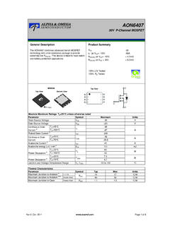
www.aosmd.comAON6407 30V P-Channel MOSFET General Description Product Summary VDS I D (at V GS = -10V) -85A R DS(ON) (at V GS = -10V) < 4.5m Ω R DS(ON) (at V GS = -6V) < 6.0m Ω 100% UIS Tested 100% R g Tested Symbol Drain-Source Voltage VDS-30 The AON6407 combines advanced trench MOSFET

30V P-Channel MOSFET
aosmd.comAO4801A TYPICAL ELECTRICAL AND THERMAL CHARACTERISTICS 17 5 2 10 0 18 40 0 5 10 15 20 0 0.5 1 1.5 2 2.5 3-V GS (Volts) Figure 2: Transfer Characteristics (Note E)-I
V R D -30V = -10V -3
www.irf.com2 www.irf.com PROVISIONAL Parameter Min. Typ. Max. Units Conditions IS Continuous Source Current MOSFET symbol (Body Diode) showing the ISM Pulsed Source Current integral reverse (Body Diode) p-n junction diode. VSD Diode Forward Voltage ––– ––– -1.2 V TJ = 25°C, IS = -1.3A, VGS = 0V trr Reverse Recovery Time ––– 17 26 ns TJ = 25°C, IF = -1.3A

NISB 3600 Quick Reference Guide Ver A. (P/N: …
files.nexcom.comNISB 3600 Quick Reference Guide Ver A. (P/N: 60177A0267X00) CON1 JP4 JP5 JP6 J11 JP1 JP3 FAN1 J1 J3 J4 FAN2 Power Switch Cfast Display Port USB 3.0 Remote Power on/off Switch 9-30V Input

IRHNJ57Z30 RADIATION HARDENED JANSR2N7479U3 …
www.irf.comwww.irf.com 3 Pre-Irradiation IRHNJ57Z30, JANSR2N7479U3 Table 1. Electrical Characteristics @ Tj = 25°C, Post Total Dose Irradiation Parameter Up to 500K Rads(Si)1 1000K Rads (Si) 2 Units Test Conditions Min Max Min Max

30V N-ChannelNexFET™ Power MOSFETs
www.ti.comCSD17304Q3 SLPS258A – FEBRUARY 2010– REVISED OCTOBER 2010 www.ti.com These devices have limited built-inESD protection. The leads should be shorted together or …
30V, N-ChannelNexFET™ Power MOSFETs
www.ti.comCSD17501Q5A SLPS303B – DECEMBER 2010– REVISED SEPTEMBER 2012 www.ti.com These devices have limited built-inESD protection. The leads should be …
RFID Specifications Technical Data
literature.rockwellautomation.comRockwell Automation Publication 56RF-TD001D-EN-P - December 2018 5 High-frequency EtherNet/IP Interface Block Table 6 - General Specifications Attribute 56RF-IN …