Transcription of CS5171 - Boost Regulators, 1.5 A, 280 kHz/560 kHz
1 DATA Semiconductor Components Industries, LLC, 2010 August, 2021 Rev. 251 Publication Order Number: CS5171 /D Boost Regulators, A,280 kHz/560 kHzCS5171, CS5172, CS5173,CS5174 The CS5171 /2/3/4 products are 280 kHz/560 kHz switchingregulators with a high efficiency , A integrated switch. These partsoperate over a wide input voltage range, from V to 30 V. Theflexibility of the design allows the chips to operate in most powersupply configurations, including Boost , flyback, forward, inverting,and SEPIC. The ICs utilize current mode architecture, which allowsexcellent load and line regulation, as well as a practical means forlimiting current. Combining high frequency operation with a highlyintegrated regulator circuit results in an extremely compact powersupply solution.
2 The circuit design includes provisions for featuressuch as frequency synchronization, shutdown, and feedback controlsfor either positive or negative voltage regulation. These parts arepin to pin compatible with LT1372 NumberFrequencyFeedback Voltage PolarityCS5171280 kHzpositiveCS5172280 kHznegativeCS5173560 kHzpositiveCS5174560 kHznegativeFeatures Integrated Power Switch: A Guaranteed Wide Input Range: V to 30 V high Frequency Allows for Small Components Minimum External Components Easy External Synchronization Built in Overcurrent Protection Frequency Foldback Reduces Component Stress During anOvercurrent Condition Thermal Shutdown with Hysteresis Regulates Either Positive or Negative Output Voltages Shut Down Current: 50 mA Maximum Pin to Pin Compatible with LT1372/1373 Wide Temperature Range Industrial Grade: 40 C to 125 C Commercial Grade.
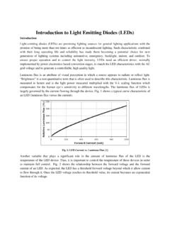
3 0 C to 125 C These Devices are Pb Free, Halogen Free/BFR Free and are RoHSCompliant517xy = Device Code x= 1, 2, 3, or 4y= E, GA= Assembly LocationL= Wafer LotY= YearW= Work WeekG= Pb Free PackageORDERING INFORMATIONCS5171/3CS5172/4 SOIC 8D SUFFIXCASE 751 VCCSS1517xyALYWG8 AGNDTestPGNDFBVSWVCVCCSS1517xyALYWG8 AGNDNFBPGNDTestVSWVCSee detailed ordering and shipping information in thepackage dimensions section on page 20 of this data DIAGRAM ANDPIN CONNECTIONSCS5171, CS5172, CS5173, + CS5171 /312345678 VOUTL15 VC322 mFVCFBTestSSVCCAGNDPGNDVSW+MBRS120T3D122 mHC222 VR15 mFFigure 1. Applications DiagramMAXIMUM RATINGSR atingValueUnitJunction Temperature Range, TJ 40 to +150 CStorage Temperature Range, TSTORAGE 65 to +150 CPackage Thermal Resistance, Junction to Case, RqJCJunction to Ambient, RqJA45165 C/W C/WLead Temperature Soldering: Reflow (Note 1)260 Peak CESD, Human Body exceeding those listed in the Maximum Ratings table may damage the device.
4 If any of these limits are exceeded, device functionalityshould not be assumed, damage may occur and reliability may be 60 second maximum above 183 RATINGS Pin NamePin SymbolVMAXVMINISOURCEISINKIC Power InputVCC35 V VN/A200 mAShutdown/SyncSS30 V mALoop V V10 mA10 mAVoltage Feedback InputFB( CS5171 /3 only)10 V mANegative Feedback Input(transient, 10 ms)NFB(CS5172/4 only) 10 V10 mATest V mAPower V V4 A10 mAAnalog GroundAGND0 V0 VN/A10 mASwitch InputVSW40 V V10 ACS5171, CS5172, CS5173, CHARACTERISTICS ( V< VCC < 30 V; Industrial Grade: 40 C < TJ < 125 C; Commercial Grade: 0 C < TJ < 125 C; For all CS5171 /2/3/4 specifications unless otherwise stated.)CharacteristicTest ConditionsMinTypMaxUnitPositive and Negative Error AmplifiersFB Reference Voltage ( CS5171 /3 only)VC tied to FB.
5 Measure at Reference Voltage (CS5172/4 only)VC = V Input Current ( CS5171 /3 only)FB = VREF Input Current (CS5172/4 only)NFB = NVREF 16 10 Reference Voltage Line Regulation( CS5171 /3 only)VC = FB Reference Voltage Line Regulation(CS5172/4 only)VC = V Error Amp TransconductanceIVC = 25 mA300550800mMhoNegative Error Amp TransconductanceIVC = 5 mA115160225mMhoPositive Error Amp Gain(Note 2)200500 V/VNegative Error Amp Gain(Note 2)100180320V/VVC Source CurrentFB = V or NFB = V, VC = V255090mAVC Sink CurrentFB = V or NFB = V, VC = V2006251500mAVC high Clamp VoltageFB = V or NFB = V; VC sources 25 Low Clamp VoltageFB = V or NFB = V, VC sinks 25 ThresholdReduce VC from V until switching Operating FrequencyCS5171/2, FB = 1 V or NFB = V230280310kHzReduced Operating FrequencyCS5171/2, FB = 0 V or NFB = 0 V3052120kHzMaximum Duty CycleCS5171/29094 %Base Operating FrequencyCS5173/4, FB = 1 V or NFB = V460560620kHzReduced Operating FrequencyCS5173/4.
6 FB = 0 V or NFB = 0 V60104160kHzMaximum Duty CycleCS5173/48290 %NFB Frequency Shift ThresholdFrequency drops to reduced operating frequency Frequency Shift ThresholdFrequency drops to reduced operating ShutdownSync RangeCS5171/2320 500kHzSync RangeCS5173/4640 1000kHzSync Pulse Transition ThresholdRise time = 20 VSS Bias CurrentSS = 0 VSS = V 15 Threshold V VCC 12 V12 V < VCC 30 V12128036350200msms2. Guaranteed by design, not 100% tested in , CS5172, CS5173, CHARACTERISTICS ( V< VCC < 30 V; Industrial Grade: 40 C < TJ < 125 C; Commercial Grade: 0 C < TJ < 125 C; For all CS5171 /2/3/4 specifications unless otherwise stated.)CharacteristicUnitMaxTypMinTest ConditionsPower SwitchSwitch Saturation VoltageISWITCH = A, (Note 3)ISWITCH = A, 0 C TJ 85 CISWITCH = A, 40 C TJ 0 CISWITCH = 10 mA Current Limit50% duty cycle, (Note 3)80% duty cycle, (Note 3) Pulse WidthFB = 0 V or NFB = 0 V, ISW = A, (Note 3)200250300nsDICC/ V VCC 12 V, 10 mA ISW A12 V < VCC 30 V, 10 mA ISW V VCC 12 V, 10 mA ISW A, (Note 3)12 V < VCC 30 V, 10 mA ISW A, (Note 3)
7 10 17 3010030100mA/AmA/AmA/AmA/ASwitch LeakageVSW = 40 V, VCC = 0V CurrentISW = 0 Mode CurrentVC < V, SS = 0 V, V VCC 12 VVC < V, SS = 0 V, 12 V VCC 30 V 12 60100mAMinimum Operation Input VoltageVSW switching, maximum ISW = 10 mA Shutdown(Note 3)150180210 CThermal Hysteresis(Note 3) 25 C3. Guaranteed by design, not 100% tested in parametric performance is indicated in the Electrical Characteristics for the listed test conditions, unless otherwise noted. Productperformance may not be indicated by the Electrical Characteristics if operated under different PIN DESCRIPTIONP ackagePin #PinSymbolFunction1 VCLoop compensation pin. The VC pin is the output of the error amplifier and is used for loop compensation,current limit and soft start.
8 Loop compensation can be implemented by a simple RC network as shown in theapplication diagram on page 2 as R1 and ( CS5171 /3only)FBPositive regulator feedback pin. This pin senses a positive output voltage and is referenced to V. Whenthe voltage at this pin falls below V, chip switching frequency reduces to 20% of the nominal (CS5172/4)3CS5171/3)TestThese pins are connected to internal test logic and should either be left floating or tied to ground. Connectionto a voltage between 2 V and 6 V shuts down the internal oscillator and leaves the power switch (CS5172/4)NFBN egative feedback pin. This pin senses a negative output voltage and is referenced to V. When thevoltage at this pin goes above V, chip switching frequency reduces to 20% of the nominal and shutdown pin.
9 This pin may be used to synchronize the part to nearly twice the basefrequency. A TTL low will shut the part down and put it into low current mode. If synchronization is not used,this pin should be either tied high or left floating for normal power supply pin. This pin supplies power to the part and should have a bypass capacitor connected , CS5172, CS5173, PIN DESCRIPTIONP ackagePin #FunctionPinSymbol6 AGNDA nalog ground. This pin provides a clean ground for the controller circuitry and should not be in the path oflarge currents. The output voltage sensing resistors should be connected to this ground pin. This pin isconnected to the IC ground. This pin is the ground connection for the emitter of the power switching transistor.
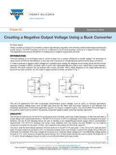
10 Connectionto a good ground plane is current switch pin. This pin connects internally to the collector of the power switch. The open voltageacross the power switch can be as high as 40 V. To minimize radiation, use a trace as short as + + + VCCSSNFBFBAGNDP ositiveError AmpCS5172/4onlyCS5171/3onlyNegativeError AmpPWM VRegulatorDelayTimerSyncShutdownOscillat orFrequencyShift 5:1 SPWML atchRQDriverSwitch63 mW V V V250 k200 VVC 5 Figure 2. Block DiagramCS5171, CS5172, CS5173, PERFORMANCE CHARACTERISTICS0 Temperature ( C)Figure 3. ICC (No Switching) vs. TemperatureCurrent (mA) = 30 = 12 VVCC = V0 Temperature ( C)Figure 4. DICC/ DIVSW vs. Temperature (mA/A)7060504030201050100 VCC = 30 VVCC = 12 VVCC = VISW = A0 ISW (mA)Figure 5.