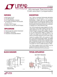
Transcription of LTC6804-1/LTC6804-2 – Multicell Battery Monitors
1 ltc6804 -1/ ltc6804 -21680412fcFor more information applicaTion FeaTuresDescripTionMulticell Battery Monitors The LT C 6804 is a 3rd generation Multicell Battery stack monitor that measures up to 12 series connected Battery cells with a total measurement error of less than The cell measurement range of 0V to 5V makes the ltc6804 suitable for most Battery chemistries. All 12 cell voltages can be captured in 290 s, and lower data acquisition rates can be selected for high noise ltc6804 devices can be connected in series, permitting simultaneous cell monitoring of long, high volt-age Battery strings. Each ltc6804 has an isoSPI interface for high speed, RF-immune, local area communications. Using the ltc6804 -1, multiple devices are connected in a daisy-chain with one host processor connection for all devices. Using the ltc6804 -2, multiple devices are con-nected in parallel to the host processor, with each device individually features include passive balancing for each cell, an onboard 5V regulator, and 5 general purpose I/O lines.
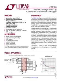
2 In sleep mode, current consumption is reduced to 4 A. The ltc6804 can be powered directly from the Battery , or from an isolated , LT, LTC, LTM, Linear Technology and the Linear logo are registered and isoSPI is a trademark of Linear Technology Corporation. All other trademarks are the property of their respective owners. Protected by patents, including 8908799, 9182428, Measurement Error vs Temperature of 5 Typical UnitsapplicaTions nMeasures Up to 12 Battery Cells in Series nStackable Architecture Supports 100s of Cells nBuilt-In isoSPI Interface: 1 Mbps Isolated Serial Communications Uses a Single Twisted Pair, Up to 100 Meters Low EMI Susceptibility and Emissions Maximum Total Measurement Error n290 s to Measure All Cells in a System nSynchronized Voltage and Current Measurement n16-Bit Delta-Sigma ADC with Frequency Program-mable 3rd Order Noise Filter nEngineered for ISO26262 Compliant Systems nPassive Cell Balancing with Programmable Timer n5 General Purpose Digital I/O or Analog Inputs.
3 Temperature or other Sensor Inputs Configurable as an I2C or SPI Master n4 A Sleep Mode Supply Current n48-Lead SSOP Package nElectric and Hybrid Electric Vehicles nBackup Battery Systems nGrid Energy Storage nHigh Power Portable EquipmentLTC6820 ltc6804 -1 MPUIP SPIIMIPAIMA680412 TA01aIPBIMBLTC6804-1 IMAIPAILPIPBIMBLTC6804-1 IMAIPBIMBIPA12S1P++++++TEMPERATURE ( C) 50 MEASUREMENT ERROR (mV) TA01b0 25050 VOLTAGE = TYPICAL UNITSLTC6804-1/ ltc6804 -22680412fcFor more information oF conTenTsFeatures ..1 Applications ..1 Typical Application .. 1 Absolute Maximum Ratings ..3 Pin Configuration ..3 Order Information ..4 Electrical Characteristics ..4 Pin Functions ..17 Block Diagram .. 20 State Diagram ..20 ltc6804 Core State Descriptions ..20isoSPI State Descriptions ..21 Power Consumption ..21 ADC Operation ..21 Data Acquisition System Diagnostics ..26 Watchdog and Software Discharge Timer ..30I2C/SPI Master on ltc6804 Using GPIOS ..31 Serial Interface Overview.
4 354-Wire Serial Peripheral Interface (SPI) Physical Layer ..362-Wire Isolated Interface (isoSPI) Physical Layer .. 36 Data Link Layer ..44 Network Layer ..44 Programming Examples ..54 Simple Linear Regulator ..58 Improved Regulator Power Efficiency ..58 Fully Isolated Power ..59 Reading External Temperature Probes ..59 Expanding the Number of Auxiliary Measurements ..60 Internal Protection Features ..60 Filtering of Cell and GPIO Inputs ..60 Cell Balancing with Internal Mosfets ..62 Cell Balancing with External Control During Cell Measurements ..62 Power Dissipation and Thermal Shutdown ..63 Method to Verify Balancing Circuitry ..63 Current Measurement with a Hall Effect Sensor ..66 Current Measurement with a Shunt Resistor ..66 Using the ltc6804 with Less Than 12 Cells ..67 Package Description ..76 Revision History ..77 Typical Application ..78 Related Parts ..78 ltc6804 -1/ ltc6804 -23680412fcFor more information MaxiMuM raTingsTotal Supply Voltage V+ to V ..75 VInput Voltage (Relative to V ) C0.
5 To C12 .. to 75V C(n) .. to MIN (8 n, 75V) S(n) .. to MIN (8 n, 75V) IPA, IMA, IPB, IMB .. to VREG + DRIVE Pin .. to 7V All Other Pins .. to 6 VVoltage Between Inputs V+ to C12 .. C(n) to C(n 1) .. to 8V S(n) to C(n 1) .. to 8V C12 to C8 .. to 25V (Note 1)pin conFiguraTionC8 to C4 .. to 25V C4 to C0 .. to 25 VCurrent In/Out of Pins All Pins Except VREG, IPA, IMA, IPB, IMB, S(n) ..10mA IPA, IMA, IPB, IMB ..30mAOperating Temperature Range LTC6804I .. 40 C to 85 C LTC6804H .. 40 C to 125 CSpecified Temperature Range LTC6804I .. 40 C to 85 C LTC6804H .. 40 C to 125 CJunction Temperature ..150 CStorage 65 C to 150 CLead Temperature (Soldering, 10sec)..300 CLTC6804-1 ltc6804 -21234567891011121314151617181920 21222324 TOP VIEWG PACKAGE48-LEAD PLASTIC SSOP484746454443424140393837363534333231 302928272625V+C12S12C11S11C10S10C9S9C8S8 C7S7C6S6C5S5C4S4C3S3C2S2C1 IPBIMBICMPIBIASSDO (NC)*SDI (NC)*SCK (IPA)*CSB (IMA)*ISOMDWDTDRIVEVREGSWTENVREF1 VREF2 GPIO5 GPIO4V V **GPIO3 GPIO2 GPIO1C0S1 TJMAX = 150 C, JA = 55 C/W *THE FUNCTION OF THESE PINS DEPENDS ON THE CONNECTION OF ISOMD ISOMD TIED TO V : CSB, SCK, SDI, SDO ISOMD TIED TO VREG: IMA, IPA, NC, NC **THIS PIN MUST BE CONNECTED TO V 123456789101112131415161718192021222324 TOP VIEWG PACKAGE48-LEAD PLASTIC SSOP484746454443424140393837363534333231 302928272625V+C12S12C11S11C10S10C9S9C8S8 C7S7C6S6C5S5C4S4C3S3C2S2C1A3A2A1A0 SDO (IBIAS)*SDI (ICMP)*SCK (IPA)*CSB (IMA)*ISOMDWDTDRIVEVREGSWTENVREF1 VREF2 GPIO5 GPIO4V V **GPIO3 GPIO2 GPIO1C0S1 TJMAX = 150 C, JA = 55 C/W *THE FUNCTION OF THESE PINS DEPENDS ON THE CONNECTION OF ISOMD ISOMD TIED TO V : CSB, SCK, SDI, SDO ISOMD TIED TO VREG.
6 IMA, IPA, ICMP, IBIAS **THIS PIN MUST BE CONNECTED TO V ltc6804 -1/ ltc6804 -24680412fcFor more information inForMaTionelecTrical characTerisTicsSYMBOLPARAMETERCONDITIONS MINTYPMAXUNITSADC DC SpecificationsMeasurement Resolutionl mV/bitADC Offset Voltage(Note 2) Gain Error(Note 2) %Total Measurement Error (TME) in Normal ModeC(n) to C(n 1), GPIO(n) to V = 0 (n) to C(n 1) = (n) to C(n 1), GPIO(n) to V = (n) to C(n 1) = (n) to C(n 1), GPIO(n) to V = (n) to C(n 1) = (n) to C(n 1), GPIO(n) to V = (n) to C(n 1), GPIO(n) to V = 1mVSum of Cells, V(CO) = V l Temperature, T = Maximum Specified Temperature 5 CVREG Pinl Pinl Supply Voltage VREGDl 1% The l denotes the specifications which apply over the full operating temperature range, otherwise specifications are at TA = 25 C.
7 The test conditions are V+ = , VREG = unless otherwise noted. TUBETAPE AND REELPART MARKING*PACKAGE DESCRIPTIONSPECIFIED TEMPERATURE RANGELTC6804IG-1#PBFLTC6804IG-1#TRPBFLTC 6804G-148-Lead Plastic SSOP 40 C to 85 CLTC6804HG-1#PBFLTC6804HG-1#TRPBFLTC6804 G-148-Lead Plastic SSOP 40 C to 125 CLTC6804IG-2#PBFLTC6804IG-2#TRPBFLTC6804 G-248-Lead Plastic SSOP 40 C to 85 CLTC6804HG-2#PBFLTC6804HG-2#TRPBFLTC6804 G-248-Lead Plastic SSOP 40 C to 125 CConsult LTC Marketing for parts specified with wider operating temperature ranges. *The temperature grade is identified by a label on the shipping container. Parts ending with PBF are RoHS and WEEE more information on lead free part marking, go to: For more information on tape and reel specifications, go to: Some packages are available in 500 unit reels through designated sales channels with #TRMPBF #orderinfoLTC6804-1/ ltc6804 -25680412fcFor more information characTerisTicsSYMBOLPARAMETERCONDITIONS MINTYPMAXUNITST otal Measurement Error (TME) in Filtered ModeC(n) to C(n 1), GPIO(n) to V = 0 (n) to C(n 1) = (n) to C(n 1), GPIO(n) to V = (n) to C(n 1) = (n) to C(n 1), GPIO(n) to V = (n) to C(n 1) = (n) to C(n 1), GPIO(n) to V = (n) to C(n 1), GPIO(n) to V = 1mVSum of Cells, V(CO) = V l Temperature, T = Maximum Specified Temperature 5 CVREG Pinl Pinl Supply Voltage VREGDl 1%Total Measurement Error (TME) in Fast ModeC(n) to C(n 1), GPIO(n) to V = 0 2mVC(n) to C(n 1), GPIO(n) to V = 4mVC(n) to C(n 1), GPIO(n) to V = (n) to C(n 1), GPIO(n) to V = (n) to C(n 1), GPIO(n) to V = 10mVSum of Cells, V(CO)
8 = V l 1%Internal Temperature, T = Maximum Specified Temperature 5 CVREG Pinl 1%VREF2 Pinl Supply Voltage VREGDl 2%Input RangeC(n), n = 1 to 12lC(n 1)C(n 1) + 5VC0l0 GPIO(n), n = 1 to 5l05 VILI nput Leakage Current When Inputs Are Not Being MeasuredC(n), n = 0 to 12l10 250nAGPIO(n), n = 1 to 5l10 250nAInput Current When Inputs Are Being MeasuredC(n), n = 0 to 12 2 AGPIO(n), n = 1 to 5 2 AInput Current During Open Wire Detectionl70100130 A The l denotes the specifications which apply over the full operating temperature range, otherwise specifications are at TA = 25 C. The test conditions are V+ = , VREG = unless otherwise noted. ltc6804 -1/ ltc6804 -26680412fcFor more information characTerisTicsSYMBOLPARAMETERCONDITIONS MINTYPMAXUNITSV oltage Reference SpecificationsVREF11st Reference VoltageVREF1 Pin, No Reference Voltage TCVREF1 Pin, No Load3ppm/ C1st Reference Voltage HysteresisVREF1 Pin, No Load20ppm1st Reference Long Term DriftVREF1 Pin, No Load20ppm/ kHrVREF22nd Reference VoltageVREF2 Pin, No Pin, 5k Load to V Reference Voltage TCVREF2 Pin, No Load10ppm/ C2nd Reference Voltage HysteresisVREF2 Pin, No Load100ppm2nd Reference Long Term DriftVREF2 Pin, No Load60ppm/ kHrGeneral DC SpecificationsIVPV+ Supply Current (See Figure 1: ltc6804 Operation State Diagram)State: Core = SLEEP, isoSPI = IDLEVREG = AVREG = AVREG = AVREG = AState: Core = STANDBY183250 Al103260 AState: Core = REFUP or MEASURE (CORE)VREG Supply Current(See Figure 1: ltc6804 Operation State diagram)State: Core = SLEEP, isoSPI = IDLEVREG = AVREG = AState: Core = STANDBY103560 Al63565 AState: Core =.
9 Core = (isoSPI)Additional VREG Supply Current if isoSPI in READY/ACTIVE StatesNote: ACTIVE State Current Assumes tCLK = 1 s, (Note 3) ltc6804 -2: ISOMD = 1, RB1 + RB2 = : ISOMD = 0, RB1 + RB2 = : ISOMD = 1, RB1 + RB2 = : ISOMD = 1, RB1 + RB2 = : ISOMD = 0, RB1 + RB2 = : ISOMD = 1, RB1 + RB2 = The l denotes the specifications which apply over the full operating temperature range, otherwise specifications are at TA = 25 C. The test conditions are V+ = , VREG = unless otherwise noted. ltc6804 -1/ ltc6804 -27680412fcFor more information characTerisTicsSYMBOLPARAMETERCONDITIONS MINTYPMAXUNITSV+ Supply VoltageTME Specifications Met (Note 6)l114055 VVREGVREG Supply VoltageTME Supply Rejection < 1 output voltageSourcing 1 A VSourcing 500 Supply Switch ON ResistanceVCELL = Thermal Shutdown Temperature 150 CVOL(WDT)Watchdog Timer Pin LowWDT Pin Sinking (GPIO)General Purpose I/O Pin LowGPIO Pin Sinking 4mA (Used as Digital Output) Timing SpecificationstCYCLE (Figure 3)
10 Measurement + Calibration Cycle Time When Starting from the REFUP State in Normal ModeMeasure 12 Cellsl212023352480 sMeasure 2 Cellsl365405430 sMeasure 12 Cells and 2 GPIO Inputsl284531333325 sMeasurement + Calibration Cycle Time When Starting from the REFUP State in Filtered ModeMeasure 12 2 12 Cells and 2 GPIO + Calibration Cycle Time When Starting from the REFUP State in Fast ModeMeasure 12 Cellsl101011131185 sMeasure 2 Cellsl180201215 sMeasure 12 Cells and 2 GPIO Inputsl142015641660 stSKEW1 (Figure 6)Skew Time. The Time Difference between C12 and GPIO2 Measurements, Command = ADCVAXFast Model189208221 sNormal Model493543576 stSKEW2 (Figure 3)Skew Time. The Time Difference between C12 and C0 Measurements, Command = ADCVFast Model211233248 sNormal Model609670711 stWAKER egulator Start-Up TimeVREG Generated from Drive Pin (Figure 28)l100300 stSLEEPW atchdog or Software Discharge TimerSWTEN Pin = 0 or DCTO[3:0] = Pin = 1 and DCTO[3:0] (Figure 1, Figures 3 to 7)Reference Wake-Up TimeState: Core =.
