3D IC INTEGRATION TECHNOLOGY …
efforts in 3D IC integration technology development by the ... semiconductor and back-end packaging assembly industry; how the industry’s growth had been planned and cultivated to arrive at the present condition. Having established such ... 3D IC INTEGRATION TECHNOLOGY DEVELOPMENT IN CHINA ...
Download 3D IC INTEGRATION TECHNOLOGY …

Information
Domain:
Source:
Link to this page:
Documents from same domain

Failure Modes in Wire bonded and Flip Chip …
www.circuitinsight.comFailure Modes in Wire bonded and Flip Chip Packages Mumtaz Y. Bora . Peregrine Semiconductor . San Diego, Ca. 92121 . mbora@psemi.com . Abstract . The growth of portable and wireless products is driving the miniaturization of packages resulting in the development of many
Solder Joint Embrittlement Mechanisms, Solutions …
www.circuitinsight.comCase Study 1 Data . A connector pin with gold over nickel finish design was hot solder dipped with Sn63Pb37 solder alloy. The gold layer was fully dissolved.

Process Control of Ionic Contamination Achieving …
www.circuitinsight.comProcess Control of Ionic Contamination Achieving 6-Sigma Criteria in The Assembly of Electronic Circuits P. Eckold [1], M. Routley[2], L. Henneken , G. Naisbitt[2], R. Fritsch[1], U. Welzel

Electrostatic Discharge (ESD), Factory Issues, …
www.circuitinsight.comElectrostatic Discharge (ESD), Factory Issues, Measurement Methods and Product Quality – Roadmaps and Solutions for 2025 to 2030 . Dipl.-Ing. Hartmut Berndt . B.E.STAT European ESD competence centre

BEST PRACTICES REFLOW PROFILING FOR LEAD-FREE SMT …
www.circuitinsight.comThe introduction of higher lead-free process temperatures and a reduction in solder paste deposit volumes require narrower process windows to optimize the reflow profile.

INVESTIGATION AND DEVELOPMENT OF TIN-LEAD AND …
www.circuitinsight.comsolder pastes, the lead-free paste would have a higher melting temperature and be more vulnerable to oxidization with the increased temperature during pre-heat and reflow.

What is Kelvin Test? - Circuit Insight
www.circuitinsight.comWhat is Kelvin Test? Rick Meraw and Todd Kolmodin, Gardien Services USA . Manfred Ludwig, Gardien Services China . Holger Kern, Gardien Services Germany

THE DYNAMICS OF LOW STRESS EPOXY CURING
www.circuitinsight.comTHE DYNAMICS OF LOW STRESS EPOXY CURING Robert L. Hubbard, Ph.D. Lambda Technologies, Inc. Morrisville, NC, USA bhubbard@microcure.com Iftikhar Ahmad, Ph.D.

Flip Chip Package Qualification of RF-IC Packages
www.circuitinsight.comFlip Chip Package Qualification of RF-IC Packages Mumtaz Y. Bora . Peregrine Semiconductor . San Diego, Ca. 92121 . mbora@psemi.com . Abstract. Quad Flat Pack No Leads (QFNs) are thermally enhanced plastic packages that use conventional copper leadframe with wire
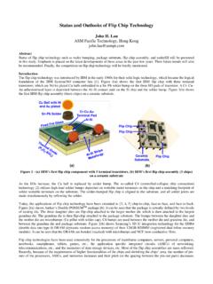
Status and Outlooks of Flip Chip Technology
www.circuitinsight.comthe organic build-up substrate, through-silicon via (TSV)-interposer, TSV-less interposer, coreless substrate, bump-on-lead (BOL), and embedded-trace-substrate (ETS) will be discussed. In order to enhance the solder joint reliability of flip chip assemblies, underfill is a must, especially for organic package substrate.
Related documents
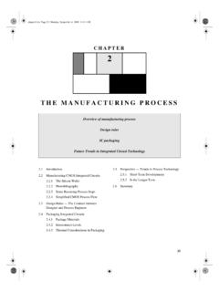
chapter2.fm Page 33 Monday, September 4, 2000 …
bwrcs.eecs.berkeley.eduIC packaging Future Trends in Integrated Circuit Technology 2.1 Introduction 2.2 Manufacturing CMOS Integrated Circuits 2.2.1 The Silicon Wafer 2.2.2 Photolithography 2.2.3 Some Recurring Process Steps ... cess that lies at the core of the semiconductor revolution. Yet, some insight in the steps ...
Semiconductor Packaging Assembly Technology - …
educypedia.karadimov.infoSemiconductor Packaging Assembly Technology Introduction This chapter describes the fundamentals of the processes used by National Semiconductor to assemble IC …

Trends, Transitions, and Inflection Points in ...
ewh.ieee.orgSemiconductor Packaging" F b 14 2018February 14, 2018 Dan Tracy, Sr. Director SEMI Industry Research & Statistics ... packaging and assembly at the wafer level ... • WB to FC • FO-WLP is a disruptive technology
DEK Semiconductor Packaging Technologies
info.dek.comDEK Semiconductor Packaging Technologies. 02 03 Lowering the Cost of ... packages – and to solve the next challenges now visible on the technology horizon. Moreover, as package outlines and interconnect dimensions continue to shrink, ... packaging and assembly markets.
WINTER 2015 - MEPTEC
meptec.orgPackaging, Assembly and Test symposium, to be held in November. 13 ANALYSIS – As the wearable technology market de - velops, there …
2016 Top Markets Report Semiconductors and …
trade.gov2016 Top Markets Report Semiconductors and Related Equipment ... 2016 ITA Semiconductors and Semiconductor Manufacturing Equipment Top Markets Report | 1 Table of Contents . ... packaging and final assembly of semiconductors and transshipments skewing the import and export data.
Electronic Packaging Technologies - Carleton …
www.doe.carleton.caElectronic Packaging Technologies 3 Issues in Electronic Packaging Mechanical analysis and testing Reliability, performance, cost, market need/timing,
Technology Trends and Future History of …
www.hitachi-chem.co.jpA 3D packaging technology for stacking semiconductor chips, on which a through silicone via (TSV) is formulated, has been increasingly investigated for its potential as the next generation high-density packaging technique.
Semiconductor Packaging Technologies for …
www.hitachi.comsemiconductor packages. This technology is especially effective for the high-pin count category. As the next-generation technology, other technologies ... Semiconductor Packaging Technologies for Miniaturization and High Pin Count 96 ... technology and assembly board interconnect design,
Semiconductor Assembly Technologies for the …
www.hitachi.comSemiconductor Assembly Technologies for the Network Era 56 for assembly technology. Cellular phones are composed of a high-frequency section, a baseband
Related search queries
Fm Page 33 Monday, September 4, Packaging, Technology, Semiconductor, Semiconductor Packaging Assembly Technology, Semiconductor Packaging, Assembly, WINTER, 2016 Top Markets Report Semiconductors and, Electronic Packaging Technologies, Technology Trends and Future History of, Packaging technology, Semiconductor Packaging Technologies for, Semiconductor Packaging Technologies for Miniaturization, Semiconductor Assembly Technologies for the, Assembly technology