Transcription of 3A Fast-Response LDO Regulator
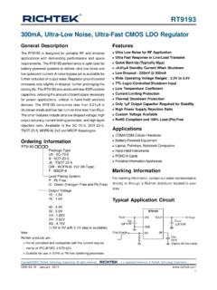
1 MIC29302A 3A Fast-Response LDO Regulator Super eta PNP is a registered trademark of Micrel, Inc. Micrel Inc. 2180 Fortune Drive San Jose, CA 95131 USA tel +1 (408) 944-0800 fax + 1 (408) 474-1000 October 3, 2014 Revision General Description The MIC29302A is a high-current, low-cost, low-dropout voltage Regulator that uses Micrel's proprietary Super eta PNP process with a PNP pass element. The 3A LDO Regulator features 450mV (full load) dropout voltage and very low ground current. Designed for high-current loads, these devices also find applications in lower current, low-dropout critical systems, where their dropout voltages and ground current values are important attributes.
2 Along with a total accuracy of 2% (over temperature, line, and load regulation) the Regulator features very fast transient recovery from input voltage surges and output load current changes. The MIC29302A has an adjustable output that can be set by two external resistors to a voltage between and 15V. In addition, the device is fully protected against overcurrent faults, reversed input polarity, reversed lead insertion, and overtemperature operation. A TTL logic enable (EN) pin is available in the MIC29302A to shutdown the Regulator .
3 When not used, the device can be set to continuous operation by connecting EN to the input (IN). The MIC29302A is available in the standard and 5-pin TO-263 and TO-252 packages with an operating junction temperature range of 40 C to +125 C. Datasheets and support documentation can be found on Micrel s website at: Features High-current capability 3A over full temperature range Low-dropout voltage of 450mV at full load Low ground current Accurate 1% guaranteed tolerance Extremely fast transient response Zero-current shutdown mode Error flag signals output out-of-regulation Adjustable output voltage Packages.
4 TO-263-5L and TO-252-5L Applications Processor peripheral and I/O supplies High-efficiency green computer systems Automotive electronics High-efficiency linear lower supplies Battery-powered equipment PC add-in cards High-efficiency post- Regulator for switching supply _____ Typical Application + = Dropout Voltagevs. Output CURRENT (A)DROPOUT VOLTAGE (mV)VIN = = 0 VTA = 25 C Micrel, Inc. MIC29302A October 3, 2014 2 Revision Ordering Information Part Number Voltage Junction Temperature Range Package MIC29302 AWU Adjustable 40 C to +125 C 5-Pin TO-263 MIC29302 AWD Adjustable 40 C to +125 C 5-Pin TO-252 Pin Configuration 5-Pin TO-263 (D2 Pak) Adjustable Voltage (U) MIC29302 AWU 5-Pin TO-252 (D-Pak) Adjustable Voltage (D) MIC29302 AWD Pin Description Pin Number TO-263 Pin Number TO-252 Pin Name Pin Function 1 1 EN Enable (Input): Active-high CMOS compatible control input.
5 Do not float. 2 2 IN INPUT: Unregulated input, +3V to +16V maximum 3, TAB 3, TAB GND GND: TAB is also connected internally to the IC s ground on both packages. 4 4 OUT OUTPUT: The Regulator output voltage 5 5 ADJ Feedback Voltage: feedback from external resistor divider. Micrel, Inc. MIC29302A October 3, 2014 3 Revision Absolute Maximum Ratings(1) Input Supply Voltage (VIN)(1) .. 20V to +20V Enable Input Voltage (VEN) .. to VIN Lead Temperature (soldering, 5 sec.) .. 260 C Power Dissipation .. Internally Limited Storage Temperature Range .. 65 C to +150 C ESD Rating all pins(3) Operating Ratings(2) Operating Junction Temperature.
6 40 C to +125 C Operating Input Voltage .. 3V to 16V Package Thermal Resistance TO-263 ( JC) .. 3 C/W TO-252 ( JC) .. 3 C/W TO-252 ( JA) .. 35 C/W TO-263 ( JA) .. 28 C/W Electrical Characteristics(4) VIN = ; IOUT = 100mA; TA = 25 C, bold values indicate 40 C TJ +125 C, unless noted. Parameter Condition Min. Typ. Max. Units Output Voltage Output Voltage Accuracy(5) 100mA IOUT 3A, (VOUT + 1V) VIN 16V 2 2 % Line Regulation IOUT = 100mA, (VOUT + 1V) VIN 16V % Load Regulation VIN = VOUT + 1V, 100mA IOUT 3A 1 % Dropout Voltage(6) IOUT = 100mA 80 200 mV IOUT = 750mA 220 IOUT = 275 IOUT = 375 630 IOUT = 430 720 IOUT = 3A 450 800 Ground Current Ground Current IOUT = 750mA, VIN = VOUT + 1V 5 20 mA IOUT = 15 IOUT = 3A 60 150 IGRNDDO Ground Pin Current @ Dropout VIN = less than specified VOUT IOUT = 10mA 2 Current Limit VOUT = 0V(7)
7 3 4 A en, Output Noise Voltage (10Hz to 100kHz CL = 10 F 400 VRMS IL = 100mA CL = 33 F 260 Ground Pin Current in Shutdown Input Voltage VIN = 16V 32 A Notes: 1. Exceeding the absolute maximum rating may damage the device. 2. The device is not guaranteed to function outside its operating rating. 3. Devices are ESD sensitive. Handling precautions recommended. Human body model, in series with 100pF. 4. Specification for packaged product only 5. Output voltage temperature coefficient is defined as the worst case voltage change divided by the total temperature change.)
8 6. Dropout voltage is defined as the input-to-output differential when output voltage drops to 99% of its normal value with VOUT + 1V applied to VIN. 7. VIN =VOUT (nominal) + 1V. For example, use VIN = for a Regulator or use 6V for a 5V Regulator . Employ pulse testing procedure for current limit. Micrel, Inc. MIC29302A October 3, 2014 4 Revision Electrical Characteristics(4) (Continued) VIN = ; IOUT = 10mA; TA = 25 C, bold values indicate 40 C TJ +125 C, unless noted. Reference Reference Voltage Note 8 V Adjust Pin Bias Current 40 nA 120 ENABLE Input Input Logic Voltage Low (OFF) V High (ON) Enable Pin Input Current VEN = 15 30 A 75 VEN = 2 4 Regulator Output Current in Shutdown Note 10 10 A 20 Notes: 8.
9 VREF VOUT VIN -1, 3V VOUT 16V, 10mA IL IFL, TJ TJmax. 9. Thermal regulation is defined as the change in the output voltage at a time T after a change in power dissipation is applied, excluding load or line regulation effects. Specifications are for a 250mA load pulse at VIN = 16V (a 4W pulse) for T = 10ms. 10. VEN , VIN 16V and VOUT = 0V. Micrel, Inc. MIC29302A October 3, 2014 5 Revision Typical Characteristics Dropout Voltage vs. Input Voltage 01002003004005000481216 INPUT VOLTAGE (V)DROPOUT VOLTAGE (mV)IOUT = 3 AIOUT = GND Pin Current vs.
10 Input VOLTAGE (V)GROUND CURRENT (mA)IOUT = 3A Adjust Pin Voltagevs. Input VOLTAGE (V)ADJ PIN VOLTAGE (V)VOUT = = 3A Adjust Pin Currentvs. Input Voltage404244460481216 INPUT VOLTAGE (V)ADJ PIN CURRENT (nA)ILOAD = 10mA Load Regulationvs. Input Voltage VOLTAGE (V)LOAD REGULATION (%)VOUT = = 10mA to 3A Short-Circuit Currentvs. Input Voltage 02468100481216 INPUT VOLTAGE (V)CURRENT LIMIT (A)VOUT = 0V Enable Pin Currentvs. Input Voltage VOLTAGE (V)ENABLE PIN CURRENT ( A)VOUT = = 10mA VEN = VIN Output Voltagevs. Input Voltage VOLTAGE (V)OUTPUT VOLTAGE (V)VOUT = = 10mA Micrel, Inc.