Transcription of LM324 - Single Supply Quad Operational Amplifiers
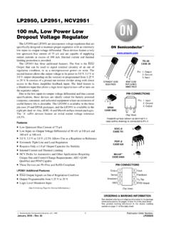
1 DATA Semiconductor Components Industries, LLC, 2016 October, 2021 Rev. 311 Publication Order Number: LM324 /DSingle Supply QuadOperational AmplifiersLM324, LM324A, LM324E,LM224, LM2902, LM2902E,LM2902V, NCV2902 The LM324 series are low cost, quad Operational Amplifiers withtrue differential inputs. They have several distinct advantages overstandard Operational amplifier types in Single Supply applications. Thequad amplifier can operate at Supply voltages as low as V or ashigh as 32 V with quiescent currents about one fifth of thoseassociated with the MC1741 (on a per amplifier basis). The commonmode input range includes the negative Supply , thereby eliminating thenecessity for external biasing components in many applications.
2 Theoutput voltage range also includes the negative power Supply Short Circuited Protected Outputs True Differential input Stage Single Supply Operation: V to 32 V Low input Bias Currents: 100 nA Maximum (LM324A) Four Amplifiers Per Package Internally Compensated Common Mode Range Extends to Negative Supply Industry Standard Pinouts ESD Clamps on the Inputs Increase Ruggedness without AffectingDevice Operation NCV Prefix for Automotive and Other Applications RequiringUnique Site and Control Change Requirements; AEC Q100 Qualified and PPAP Capable These Devices are Pb Free, Halogen Free/BFR Free and are RoHSCompliant14 SOIC 14D SUFFIXCASE 751A1 PIN CONNECTIONS8 Out 4 Inputs 4 VEE, GNDI nputs 3 Out 3910111213142 Out 1 VCCOut 2134567*)Inputs 1 Inputs 2(Top View)4231)**))*See general marking information in the device markingsection on page 11 of this data MARKING INFORMATIONSee detailed ordering and shipping information in the packagedimensions section on page 10 of this data INFORMATION114 TSSOP 14 DTB SUFFIXCASE 948 GLM324, LM324A, LM324E, LM224, LM2902, LM2902E, LM2902V, RATINGS (TA = + 25 C, unless otherwise noted.
3 RatingSymbolValueUnitPower Supply VoltagesVdcSingle SupplyVCC32 Split SuppliesVCC, VEE 16 input Differential Voltage Range (Note 1)VIDR 32 VdcInput Common Mode Voltage RangeVICR to 32 VdcOutput Short Circuit DurationtSCContinuousJunction TemperatureTJ150 CThermal Resistance, Junction to Air (Note 2)Case 646 Case 751 ACase 948GR JA118156190 C/WStorage Temperature RangeTstg 65 to +150 COperating Ambient Temperature RangeTA CLM224 25 to +85LM324, LM324A, LM324E0 to +70LM2902, LM2902E 40 to +105LM2902V, NCV2902 (Note 3) 40 to +125 Stresses exceeding those listed in the Maximum Ratings table may damage the device. If any of these limits are exceeded, device functionalityshould not be assumed, damage may occur and reliability may be Split Power All R JA measurements made on evaluation board with 1 oz.
4 Copper traces of minimum pad size. All device outputs were is qualified for automitive RATINGSR atingHBMMMUnitESD Protection at any Pin (Human Body Model HBM, Machine Model MM)NCV2902 (Note 3)LM324E, LM2902 ELM324DG/DR2G, LM2902DG/DR2 GAll Other Devices200020002002000200200100200 VVVVLM324, LM324A, LM324E, LM224, LM2902, LM2902E, LM2902V, CHARACTERISTICS (VCC = V, VEE = GND, TA = 25 C, unless otherwise noted.)LM224LM324 ALM324, LM324 ELM2902, LM2902 ELM2902V/NCV2902 CharacteristicsSymbolMinTypMaxMinTypMaxM inTypMaxMinTypMaxMinTypMaxUnitInput Offset VoltageVIOmVVCC = V to 30 VVICR = 0 V toVCC V,VO = V, RS = 0 TA = 25 C = Thigh (Note 4) 10 13TA = Tlow (Note 4) 10 10 Average TemperatureCoefficient of InputOffset Voltage VIO/ T V/ CTA = Thigh to Tlow(Notes 4 and 6) input Offset CurrentIIO = Thigh to Tlow(Note 4) 100 75 150 200 200 Average TemperatureCoefficient of InputOffset Current IIO/ T 10 10300 10 10 10 pA/ CTA = Thigh to Tlow(Notes 4 and 6) input Bias CurrentIIB 90 150 45 100 90 250 90 250 90 250nATA = Thigh to Tlow(Note 4)
5 300 200 500 500 500 input Common ModeVoltage Range(Note 5)VICRVVCC = 30 VTA = +25 C0 = Thigh to Tlow(Note 4)0 280 280 280 280 28 Differential InputVoltage RangeVIDR VCC VCC VCC VCC VCCVL arge Signal OpenLoop Voltage GainAVOLV/mVRL = k , VCC = 15 V, for Large VO Swing50100 25100 25100 25100 25100 TA = Thigh to Tlow(Note 4)25 15 15 15 15 Channel Separation10 kHz f 20 kHz, input ReferencedCS 120 120 120 120 120 dBCommon ModeRejection, RS 10 k CMR7085 6570 6570 5070 5070 dBPower SupplyRejectionPSR65100 65100 65100 50100 50100 dB4. LM224: Tlow = 25 C, Thigh = +85 CLM324/LM324A/LM324E: Tlow = 0 C, Thigh = +70 CLM2902/LM2902E: Tlow = 40 C, Thigh = +105 CLM2902V & NCV2902: Tlow = 40 C, Thigh = +125 CNCV2902 is qualified for automotive The input common mode voltage or either input signal voltage should not be allowed to go negative by more than V.
6 The upper end ofthe common mode voltage range is VCC V, but either or both inputs can go to +32 V without damage, independent of the magnitudeof Guaranteed by , LM324A, LM324E, LM224, LM2902, LM2902E, LM2902V, CHARACTERISTICS (VCC = V, VEE = GND, TA = 25 C, unless otherwise noted.)LM224LM324 ALM324, LM324 ELM2902, LM2902 ELM2902V/NCV2902 CharacteristicsSymbolMinTypMaxMinTypMaxM inTypMaxMinTypMaxMinTypMaxUnitOutput Voltage High LimitVOHVVCC = V, RL = k , TA = 25 VCC = 30 VRL = k (TA = Thigh to Tlow)(Note 7)26 26 26 26 26 VCC = 30 VRL = 10 k (TA = Thigh to Tlow)(Note 7)2728 2728 2728 2728 2728 output Voltage Low Limit, VCC = V, RL = 10 k ,TA = Thigh to Tlow(Note 7)VOL Source Current(VID = + V, VCC = 15 V)IO +mATA = 25 C2040 2040 2040 2040 2040 TA = Thigh to Tlow(Note 7)1020 1020 1020 1020 1020 output Sink CurrentIO mA(VID = V, VCC = 15 V) TA = 25 C1020 1020 1020 1020 1020 TA = Thigh to Tlow(Note 7) (VID = V, VO = 200 mV, TA = 25 C)
7 1250 1250 1250 AOutput Short Circuitto Ground(Note 8)ISC 4060 4060 4060 4060 4060mAPower Supply Current(TA = Thigh to Tlow)(Note 7)ICCmAVCC = 30 VVO = 0 V, RL = = V,VO = 0 V, RL = LM224: Tlow = 25 C, Thigh = +85 CLM324/LM324A/LM324E: Tlow = 0 C, Thigh = +70 CLM2902/LM2902E: Tlow = 40 C, Thigh = +105 CLM2902V & NCV2902: Tlow = 40 C, Thigh = +125 CNCV2902 is qualified for automotive The input common mode voltage or either input signal voltage should not be allowed to go negative by more than V. The upper end ofthe common mode voltage range is VCC V, but either or both inputs can go to +32 V without damage, independent of the magnitudeof parametric performance is indicated in the Electrical Characteristics for the listed test conditions, unless otherwise noted.
8 Productperformance may not be indicated by the Electrical Characteristics if operated under different , LM324A, LM324E, LM224, LM2902, LM2902E, LM2902V, 1. Representative Circuit Diagram(One Fourth of Circuit Shown)OutputBias CircuitryCommon to kQ25Q2240 kQ24Q23Q1225+- LM324 , LM324A, LM324E, LM224, LM2902, LM2902E, LM2902V, DESCRIPTIONThe LM324 series is made using four internallycompensated, two stage Operational Amplifiers . The firststage of each consists of differential input devices Q20 andQ18 with input buffer transistors Q21 and Q17 and thedifferential to Single ended converter Q3 and Q4. The firststage performs not only the first stage gain function but alsoperforms the level shifting and transconductance reductionfunctions.
9 By reducing the transconductance, a smallercompensation capacitor (only pF) can be employed, thussaving chip area. The transconductance reduction isaccomplished by splitting the collectors of Q20 and feature of this input stage is that the input commonmode range can include the negative Supply or ground, insingle Supply operation, without saturating either the inputdevices or the differential to Single ended converter. Thesecond stage consists of a standard current source loadamplifier 2. Large Signal Voltage Follower ResponseVCC = 15 VdcRL = k TA = 25 V/DIVEach amplifier is biased from an internal voltageregulator which has a low temperature coefficient thusgiving each amplifier good temperature characteristics aswell as excellent power Supply SupplySplit V to VCC(max) V to VCC(max) V to VEE(max)Figure 3.
10 CAPACITANCE (pF)Phase MarginFigure 4. Gain and Phase Margin1000706050403020100 GAIN MARGIN (dB)PHASE MARGIN ( )Gain MarginLM324, LM324A, LM324E, LM224, LM2902, LM2902E, LM2902V, , output VOLTAGE RANGE (V)ppVO, output VOLTAGE (mV) , FREQUENCY (kHz) , TIME ( s) , POWER Supply VOLTAGE (V)VCC, POWER Supply VOLTAGE (V) , POWER Supply CURRENT (mA)CCI , input BIAS CURRENT (nA)IBVCC = 30 VVEE = GNDTA = 25 CCL = 50 pFInputOutputV , input VOLTAGE (V)I18 161412 101214 161820 VCC/VEE, POWER Supply VOLTAGES (V) PositiveNegativeTA = 25 CRL = RRL = k VCC = 15 VVEE = GNDGain = -100RI = k RF = 100 k Figure 5. input Voltage RangeFigure 6. Open Loop k10 k100 Mf, FREQUENCY (Hz)A , LARGE-SIGNALVOLOPEN LOOP VOLTAGE GAIN (dB)VCC = 15 VVEE = GNDTA = 25 CFigure 7.
