Transcription of NCP4318 - Advanced Synchronous Rectifier Controller for ...
1 DATA Semiconductor Components Industries, LLC, 2020 December, 2021 Rev. 51 Publication Order Number: NCP4318 /DAdvanced SynchronousRectifier Controller for LLCR esonant ConverterNCP4318 NCP4318 is an Advanced Synchronous rectification (SR) controllerfor LLC resonant converter with minimum external components. Ithas two gate drivers for driving the SR MOSFETs rectifying theoutputs of the secondary transformer windings. The two gate drivershave their own drain and source sensing pins and operateindependently of each other. The Advanced adaptive dead time controlcompensates the voltage across parasitic inductance to minimize thebody diode conduction and maximize the system efficiency.
2 Theadvanced turn off control algorithm allows stable SR operation overentire load range. NCP4318 has two versions of pin assignment NCP4318A, NCP4318B, and two types of package SOIC 8 andSOIC 8 Mixed Mode SR Turn off Control Anti Shoot through Control for Reliable SR Operation 200 V rated Drain Sensing and Dedicated Source Sensing Pins Advanced Adaptive Dead Time Control SR Current Inversion Detection Adaptive Minimum Turn on Time for Noise Immunity SR Conduction Time Increase Rate Limitation Multi level Turn off Threshold Voltage Adaptive Gate Voltage (10 V, 6 V) Low Operating Current (100 mA)
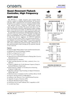
3 In Green Mode Soft Start with 0 V / 6 V Gate Output Voltage Short Turn on and Turn off Delay Time (30 ns / 30 ns) High Gate Sourcing and Sinking Current ( A / A) Wide Operating Supply Voltage Range from V to 35 V Wide Operating Frequency Range (22 kHz to 500 kHz) SOIC 8 and SOIC 8 EP Packages These Devices are Pb Free and are RoHS CompliantApplications High Power Density Adapters Large Screen LED TV and OLED TV Power Supplies High Efficiency Desktop and Server Power Supplies Networking and Telecom Power Supplies High Power LED LightingPIN CONNECTIONSSee detailed ordering, marking and shipping information onpage 3 of this data INFORMATIONMARKING DIAGRAMSOIC 8, 150 milsCASE 751 BDU= Pin Layout, A and BV= Frequency, H: High, L.
4 LowWX = Additional IPT OptionA= Assembly LocationWL = Wafer Lot TraceabilityYYWW = Date CodeNCP4318 UVWXAWLYYWW18 NCP4318 AXXGATE1 GNDVS1VD1 GATE2 VDDVD2VS2 NCP4318 BXXGATE1 GNDVD1VS1 GATE2 VDDVD2VS2(Top View)SOIC 8 EPCASE 1. Typical Application Schematic of NCP4318Q1 LrCrQ2 VOLpCinCORONCP4318AG1 GNDVS1VD1G2 VDDVD2VS2 OptionalOptionalVACB ridgeDiodeEMIF ilterShuntRegulatorLLCC ontrollerRoffset2 PFCS tageM1M2 Roffset1 Figure 2. Internal Block Diagram of NCP4318 VDDA daptiveturn ondelayQQSETCLRDVTH ONTurn onVD1 Turn offGNDVTH OFF1 VTH HGHVD1_HIGHDLY_EN1 IOFFSET1 AdaptiveTmin onGATECLAMPIOFFSET1 VTH OFF1VD1 HGHSRCINV1 GREEN MODESRCOND1.
5 2VD1_HGHVG1 SRConductionSRCOND1 GREENVDD GATE ON/VDD GATE OFFSOFTSTARTSRCOND1 SRCOND2SS_7 VGREENRUNRUNA daptiveturn ondelayQQSETCLRDVTH ONTurn onTurn offVTH OFF2 VTH HGHVD2_HIGHDLY_EN2 IOFFSET2 AdaptiveTmin onAdaptivedead timecontrolIOFFSET2 VTH OFF2VD2 HGHSRCINV2VG2 SRConductionSRCOND2 RUNVS1 GATE1VD2VS2 GATE2SR Current Inversion detectVD1VD2 SRCINV1 DLY_EN1 DLY_EN2 SRCINV2 Adaptivedead timecontrolGATECLAMPA daptiveVGATEP rotectionsGREENA daptiveVGATEVGATEC ontrolVTH DESCRIPTIONPin NumberNameDescriptionNCP4318 ANCP4318B11 GATE1 Gate drive output for SR MOSFET122 GNDG round34VS1 Synchronous Rectifier source sense input for SR143VD1 Synchronous Rectifier drain sense input.
6 IOFFSET1 current source flows out of the VD1pin such that an external series resistor can be used to adjust the Synchronous rectifi-er turn off threshold. The IOFFSET1 current source is turned off when VDD is under voltage or when switching is disabled in green mode55VS2 Synchronous Rectifier source sense input for SR266VD2 Synchronous Rectifier drain sense input. IOFFSET2 current source flows out of the VD2pin such that an external series resistor can be used to adjust the Synchronous rectifi-er turn off threshold. The IOFFSET2 current source is turned off when VDD is under voltage or when switching is disabled in green mode77 VDDS upply Voltage88 GATE2 Gate drive output for SR MOSFET2 ORDERING INFORMATIONO rdering CodeDevice MarkingPackageShipping NCP4318 AHDDR2 GNCP4318 AHDSOIC 8(Pb Free)2500 / Tape & ReelNCP4318 AHJDR2 GNCP4318 AHJNCP4318 ALCDR2 GNCP4318 ALCNCP4318 ALKDR2 GNCP4318 ALKNCP4318 ALLDR2 GNCP4318 ALLNCP4318 ALSDR2 GNCP4318 ALSNCP4318 BLCDR2 GNCP4318 BLCNCP4318 ALFPDR2G NCP4318 ALFPSOIC 8 EP(Pb Free)
7 For information on tape and reel specifications, including part orientation and tape sizes, please refer to our Tape and Reel Packaging Specifications Brochure, BRD8011/D. In development. Available upon RATINGSS ymbolRatingValueUnitVDDP ower Supply Input Pin Voltage to 37 VVD1, VD2 Drain Sense Input Pin Voltage 4 to 200 VVGATE1,VGATE2 Gate Drive Output Pin Voltage to 17 VVS1, VS2 Source Sense Input Pin Voltage to DYN,VS2 DYNS ource Sense Input Pin Dynamic Voltage (Pulse Width = 200 ns) 4 to Dissipation (TA = 25 C)SOIC 8 SOIC 8 Junction Temperature 40 to 150 CTSTGS torage Temperature Range 60 to 150 CTLLead Temperature (Soldering, 10 Seconds)
8 260 CESDE lectrostatic Discharge CapabilityHuman Body Model,ANSI / ESDA / JEDEC JS 001 2012(except VD1, VD2 pin)3kVHuman Body Model,VD1 GND, VD2 GND pin to pin with 330 pF (Note 2)capacitance on VD1 and VD2 pin2 Charged Device Model, JESD22 C1011 Stresses exceeding those listed in the Maximum Ratings table may damage the device. If any of these limits are exceeded, device functionalityshould not be assumed, damage may occur and reliability may be All voltage values are with respect to the GND The capacitance can be replaced by COSS of CHARACTERISTICSS ymbolRatingValueUnitRqJAThermal Resistance, Junction to 8 (Note 3)SOIC 8 EP (Note 4)16540 C/WRyJTThermal Characterization Parameter between Junction and the Center of the Top of the 8 (Note 3)SOIC 8 EP (Note 4)224 C/W3.
9 JEDEC standard: JESD51 2 (still air natural convection) and JESD51 3 (1s0p).4. JEDEC standard: JESD51 2 (still air natural convection) and JESD51 7 (2s2p) with an additional 1 oz 1 in2 copper OPERATING CONDITIONSS ymbolRatingMinMaxUnitVDDVDD Pin Supply Voltage to GND (Note 5)035 VVD1, VD2 Drain Sense Input Pin Voltage , VS2 Source Sense Input Pin Voltage Junction Temperature 40+125 CFunctional operation above the stresses listed in the Recommended Operating Ranges is not implied. Extended exposure to stresses beyondthe Recommended Operating Ranges limits may affect device Allowable operating supply voltage VDD can be limited by the power dissipation of NCP4318 related to switching frequency, load capacitanceand ambient CHARACTERISTICS (VDD = 12 V and TJ = 40 C to 125 C unless otherwise specified.)
10 SymbolParameterTest ConditionsMinTypMaxUnitSUPPLY VOLTAGE AND CURRENT SECTIONVDD ONTurn on ThresholdVDD rising with V / 1 ms OFFTurn off ThresholdVDD < VDD VVDD GATE ONSR Gate Enable Threshold VoltageVDD > VDD GATE ON GATE OFFSR Gate Disable Threshold Voltage(Note 6)VDD < VDD GATE VIDD OP1 Operating CurrentfSW = 100 kHz, CGATE = 1 nF 810mAIDD OP0 Operating CurrentfSW = 100 kHz, CGATE = 0 nF 6mAIDD STARTS tart up CurrentVDD = VDD ON V 100mAIDD GREENO perating Current in Green ModeVDD = 12 V (no VD1/2 switching) GREEN1 enable at TJ = 25 CExcluding ALFP. 100210mAhSS SKIPN umber of VD1/2 Alternative Switching for Soft Start SkippingVD1/2 falling lower than VTH ON & VD1/2rising higher than VTH HGH & No GATE output at fSW = 200 kHz, CGATE = 0 nF 255 CycleDRAIN VOLTAGE SENSING SECTIONVOSIC omparator Input Offset Voltage(Note 6) 101mVIDRAIN LKGD rain Pin Leakage CurrentVD1/2 = 200 V 1mAVTH ONTurn on Threshold (Note 6)ROFFSET = 0 W (includes comparator input offset voltage)