Transcription of PE42525 and PE426525 Performance Optimization
1 PE42525 and PE426525 Performance OptimizationApplication Note 66 2015-2017, Peregrine Semiconductor Corporation. All rights reserved. Headquarters: 9380 Carroll Park Drive, San Diego, CA, 92121 Application NoteDOC-81384-2 (08/2017) application note provides the recommended landing pattern and assembly process for achieving optimum Performance with the PE42525 and PE426525 . The PE42525 and PE426525 are flip-chip, single-pole double-throw (SPDT) switches that support a wide frequency range from 9 kHz to 60 GHz. The PE42525 is suited for test and measurement (T&M), microwave backhaul, and radar and military communications (mil-comm) applications. The PE426525 is ideal for applications that require extended temperature support in the 55 C to +125 C range, such as harsh industrial applications.
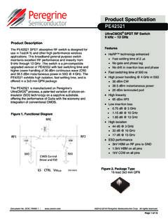
2 IntroductionPE42525 and PE426525 are the first 60 GHz millimeter-wave switches to harness the high-frequency Performance of UltraCMOS . Monolithic microwave integrated circuit (MMIC) design techniques are used to achieve unprecedented Performance in the K and Ka microwave and millimeter-wave bands. Achieving dB of insertion loss and greater than 37 dB of isolation at 50 GHz, the PE42525 and PE426525 reflective SPDT switches deliver the same high-power, high-linearity Performance for which Peregrine s UltraCMOS technology is historically OverviewThe PE42525 and PE426525 are flip-chip SPDT switches that use lead-free solder ball technology to provide the signal and ground interconnect. Solder reflow profiles common to lead-free surface-mount device (SMD) assembly can be readily used to achieve uniform and reliable 1 shows the pin configuration for the PE42525 and PE426525 .
3 Table 1 provides detailed pin descriptions. To ease routing and manufacturing, the pin configuration maintains a minimum of 500 m ( mm) pitch between all unique signal pads. Application Note 66PE42525/ PE426525 OptimizationPage 2 DOC-81384-2 (08/2017) PatternsThe PE42525 and PE426525 are configured with a mm, or 500 m, minimum ball pitch. Thin film technologies can readily meet the line width and spacing critical dimensions (CDs) of 100 m or less. Other thick film and PCB processes, by comparison, generally require significantly less stringent CDs to achieve reasonable and consistent manufacturing yields. The comparatively wide 500 m ball pitch supports large CD requirements and allows the die to be assembled directly to RF optimum microwave Performance , specific metalization and via patterns are defined and implemented to provide measured results for the PE42525 and PE426525 .
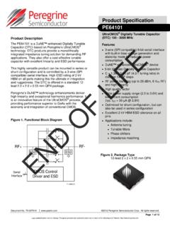
4 These recom-mended layouts can be downloaded from the Peregrine Semiconductor website at Figure 1 Pin Configuration (Bumps Up)(*)Note: *Drawing is not drawn to 1 Pin DescriptionsPin #Pin NameDescription1, 2, 5, 6, 8 10, 12 14, 16 19 GNDG round3V1 Control input 14V2 Control input 27RF1RF port 111 RFCRF common port15RF2RF port 213459131514161817191210876112 GNDV1V2 GNDGNDGNDGNDGNDGNDGNDGNDGNDGNDRF1RF2 GNDGNDRFCGNDA pplication Note 66PE42525/ PE426525 OptimizationDOC-81384-2 (08/2017)Page SubstrateFigure 2 and Figure 3 show two recommended metalization patterns and via placements for alumina substrate carriers on which the PE42525 and PE426525 are assembled. The first substrate carrier uses an alumina thickness of 10 mil with 8 mil diameter vias (see Figure 2).
5 Important parameters for the coplanar waveguide with ground (CPWG) transmission lines are: RF common port (RFC) transitions from a 50 input to a 65 line of length and width mil and mil, respectively. RF1 and RF2 ports transition from 50 transmission lines (width and spacing of mil and mil) to 64 lines of length and width of 8 mil and mil, substrate carrier is referenced as PRT66735. When this substrate is epoxied to a GND plane, the top GND is epoxied to the bottom GND for improving the RF probe to substrate transition for >40 GHz Performance , as was performed for characterization. A second substrate carrier using 10 mil alumina with improved RF probe to substrate transitions is the recommended metalization pattern.
6 The PRT67978, shown in Figure 3, has additional vias near the RF port edges, along with edge-wrapped features (where top GND metalization is wrap-connected to the bottom substrate metalization) to retain high-frequency Performance >40 the end application requires a different thickness alumina between 5 10 mil, the critical dimensions of line width, spacing, and via diameter can be readily scaled to accommodate specific thickness 2 PRT66735 10 mil Alumina Substrate Metalization and Via Pattern(*)Note: *Used for characterization and sample OutlineMetalization PatternVia LocationsSolder MaskBall Center PointPE42525 Die OutlineApplication Note 66PE42525/ PE426525 OptimizationPage 4 DOC-81384-2 (08/2017) Performance can be affected by metalization and via patterns.
7 Figure 4, for example, shows changes in insertion loss levels due to grounding differences near the RF probe transi-tions for the PRT66735. For comparison, the substrate PRT67978 used for present sampling of the PE42525 and PE426525 is also shown. The epoxied PRT66735 substrate and edge-wrapped PRT67978 substrate eliminate insertion ripple for frequencies over 40 3 PRT67978 10 mil Alumina Substrate Metalization and Via Pattern (recommended)Substrate OutlineMetalization PatternVia LocationsSolder MaskBall Center PointPE42525 Die OutlineApplication Note 66PE42525/ PE426525 OptimizationDOC-81384-2 (08/2017)Page 4 Insertion Loss Performance Comparison(*)Note: *Comparison is between 10 mil alumina substrate carriers PRT66735 (with and without epoxy) and PRT67978 metal-ization and via patterns.
8 PRT67978 is the recommended pattern. PRT66735 with epoxy grounding was used for 5 Modified PRT66735 Note: *Epoxy was used to connect top metal GND to bottom GND plane for improved RF probe to substrate 102030405060 Insertion Loss (dB)Frequency (GHz)PRT66735 "Epoxied"PRT66735 "As Is"PRT67978 Application Note 66PE42525/ PE426525 OptimizationPage 6 DOC-81384-2 (08/2017) minimize unwanted wicking of individual solder balls from the local connection point, use a solder stop such as a marking, protective polymer layer, or other material recommended by the substrate manufacturer. The solder stop thickness should be 15 25 m to prevent the solder wicking from touching the face of the PE42525 facilitate accurate measurements, the line width and spacing at the edge of the RF lines in the landing pattern are configured for 150 m pitch ground-signal-ground (GSG).
9 Users can modify and integrate the landing pattern anywhere outside the die outline to align with the higher level assembly and substrate design 4003 Printed Circuit BoardMetalization and via pattern PRT61038 have been generated for a Rogers 4003 substrate. Figure 7 shows the pattern for an 8 mil board thickness. Although this board layout is configured for high-frequency SMA connectors, the basic pattern can be used to create an RF-probable PCB (see Figure 8). The measured Performance of a PE42525 that is assembled to the RF probe-able PCB and properly de-embedded performs comparably to an alumina-based 6 Assembled PE42525 on Alumina Substrate PRT67978PE42525 DIEV1 V2 Alumina substrate boardThickness: in.
10 R = Note 66PE42525/ PE426525 OptimizationDOC-81384-2 (08/2017)Page 7 PCB Rogers 4003 PRT61038 Metalization and Via PatternsFigure 8 PCB Rogers 4003 Evaluation Board (*)Note: *Based on PRT61038 metalization and via Note 66PE42525/ PE426525 OptimizationPage 8 DOC-81384-2 (08/2017) addition to the 50 transmission line width and spacing, the dimensions of the thinner lines right at the PE42525 SPDT RF ports must also be considered. The RFC port transitions from a 50 line to a line length and width of 21 mil and 6 mil (Z = 75 ), respectively. The two RF ports, RF1 and RF2, transition from a 50 line to a line length and width of mil and 6 mil (Z = 75 ), respectively. These parameters serve as alternate matching impedances that can yield similar results if the transmission line impedances used for the alumina substrate are used for the PCB.